SNVS174I February   2003  – February 2015 LP3852 , LP3855

PRODUCTION DATA.  

  1. Features
  2. Applications
  3. Description
  4. Simplified Schematics
  5. Revision History
  6. Voltage Options
  7. Pin Configuration and Functions
  8. Specifications
    1. 8.1 Absolute Maximum Ratings
    2. 8.2 ESD Ratings
    3. 8.3 Recommended Operating Conditions
    4. 8.4 Thermal Information
    5. 8.5 Electrical Characteristics
    6. 8.6 Typical Characteristics
  9. Detailed Description
    1. 9.1 Overview
    2. 9.2 Functional Block Diagrams
    3. 9.3 Feature Description
      1. 9.3.1 SENSE Pin
      2. 9.3.2 SHUTDOWN (SD) Operation
      3. 9.3.3 Dropout Voltage
      4. 9.3.4 Reverse Current Path
      5. 9.3.5 Short-Circuit Protection
      6. 9.3.6 ERROR Flag Operation
    4. 9.4 Device Functional Modes
      1. 9.4.1 Operation with VOUT(TARGET) + 0.1 V ≤ VIN ≤ 7 V
      2. 9.4.2 Operation With SD Pin Control
  10. 10Application and Implementation
    1. 10.1 Application Information
    2. 10.2 Typical Applications
      1. 10.2.1 Design Requirements
      2. 10.2.2 Detailed Design Procedure
        1. 10.2.2.1 External Capacitors
          1. 10.2.2.1.1 Input Capacitor
          2. 10.2.2.1.2 Output Capacitor
        2. 10.2.2.2 Operation with Ceramic Output Capacitors
        3. 10.2.2.3 Selecting A Capacitor
        4. 10.2.2.4 Capacitor Characteristics
          1. 10.2.2.4.1 Ceramic
          2. 10.2.2.4.2 Tantalum
          3. 10.2.2.4.3 Aluminum
        5. 10.2.2.5 Turnon Characteristics For Output Voltages Programmed to 2 V or Below
        6. 10.2.2.6 Output Noise
      3. 10.2.3 Application Curves
  11. 11Power Supply Recommendations
  12. 12Layout
    1. 12.1 Layout Guidelines
    2. 12.2 Layout Example
    3. 12.3 RFI and/or EMI Susceptibility
    4. 12.4 Power Dissipation/Heatsinking
      1. 12.4.1 Heatsinking TO-220 Package
      2. 12.4.2 Heatsinking TO-263 Package
  13. 13Device and Documentation Support
    1. 13.1 Related Links
    2. 13.2 Trademarks
    3. 13.3 Electrostatic Discharge Caution
    4. 13.4 Glossary
  14. 14Mechanical, Packaging, and Orderable Information

封装选项

机械数据 (封装 | 引脚)
散热焊盘机械数据 (封装 | 引脚)
订购信息

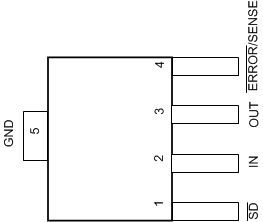
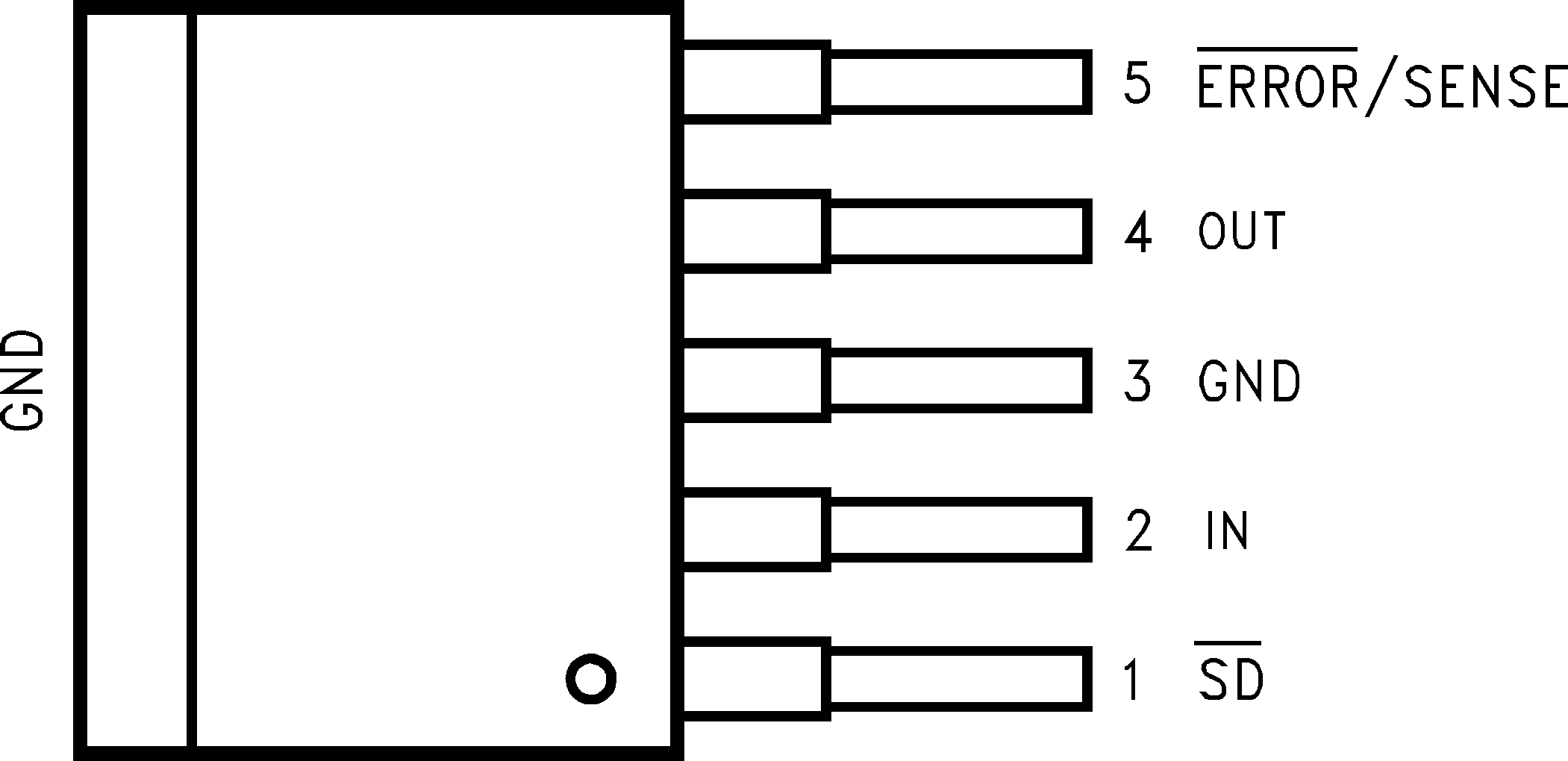
7 Pin Configuration and Functions

SOT-223 (NDC)
5 Pins
Top View
LP3852 LP3855 20031096.gif
DDPAK/TO-263 (KTT)
5 Pins
Top View
LP3852 LP3855 20031006.png
TO-220 (NDH)
5 Pins
Top View, Bent, Staggered Leads
LP3852 LP3855 20031005.png

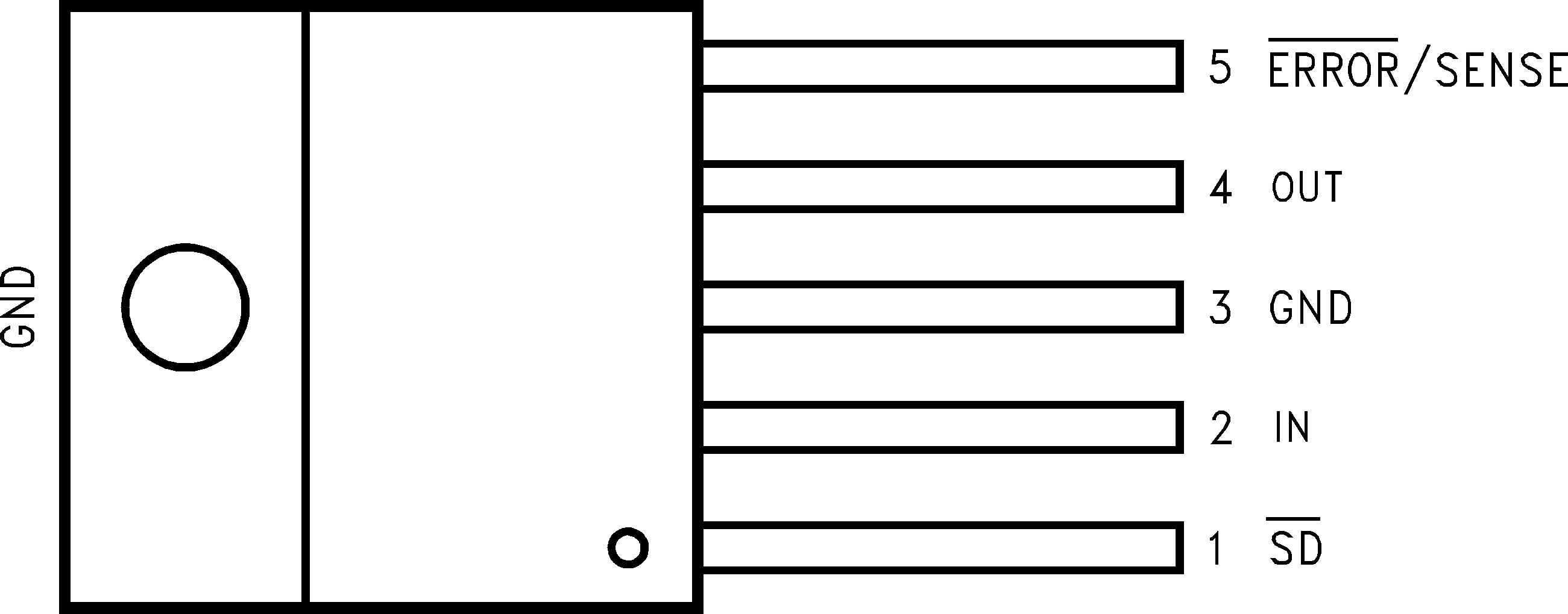
Pin Functions for SOT-223

PIN I/O DESCRIPTION
NAME LP3852 LP3855
NDC NDC
ERROR 4 N/A O ERROR flag
GND 5 5 Ground
IN 2 2 I Input supply
OUT 3 3 O Output voltage
SD 1 1 I Shutdown
SENSE N/A 4 I Remote sense pin

Pin Functions for TO-220 and TO-263

PIN I/O DESCRIPTION
NAME LP3852 LP3855
KTT/NDH KTT/NDH
ERROR 5 N/A O ERROR flag
GND 3 3 Ground
IN 2 2 I Input supply
OUT 4 4 O Output voltage
SD 1 1 I Shutdown
SENSE N/A 5 I Remote sense pin