SNVS170D October 2001 – April 2016 LP2983
PRODUCTION DATA.
- 1 Features
- 2 Applications
- 3 Description
- 4 Revision History
- 5 Pin Configuration and Functions
- 6 Specifications
- 7 Detailed Description
- 8 Application and Implementation
- 9 Power Supply Recommendations
- 10Layout
- 11Device and Documentation Support
- 12Mechanical, Packaging, and Orderable Information
7 Detailed Description
7.1 Overview
The LP2983 is a voltage regulator with optimized vertically integrated PNP designed for use with very low ESR output capacitors, excellent for low noise applications that require a clean voltage supply. The LP2983 has a wide input voltage range (16 V maximum), high accuracy (A grade 1%), and a fixed output voltage supply capable of delivering 150 mA. In addition the LP2983 device provides the following features:
- High accuracy output voltage
- Low ground current, typically 825 μA at 150-mA load and 75 μA at 1-mA load
- A sleep mode feature is available, allowing the regulator to consume only 1 µA (typical) when the ON/OFF pin is pulled low.
- Overtemperature protection and overcurrent protection circuitry designed to safeguard the device during unexpected conditions.
- Thermal protection
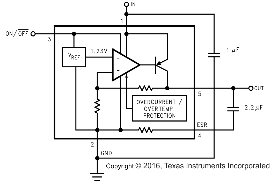
7.2 Functional Block Diagram

7.3 Feature Description
7.3.1 High-Accuracy Output Voltage
With special careful design to minimize all contributions to the output voltage error, the LP2983 distinguishes itself as a very high-accuracy output voltage micropower LDO. This includes a tight initial tolerance (typically 1.5% at 50 mA, 25°C junction temperature; also available in A grade with an accuracy of 1% under the same conditions), extremely good line regulation (0.01%/V typical), and a very low output-voltage temperature coefficient, making the part an ideal low-power voltage reference.
7.3.2 Low Ground Current
The LP2983 device uses a vertical PNP process which allows for quiescent currents that are considerably lower than those associated with traditional lateral PNP regulators, typically 825 μA at 150-mA load and 75 μA at 1-mA load.
7.3.3 Reverse Input-Output Voltage
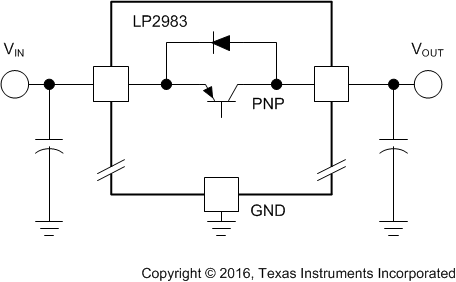
The internal PNP power transistor used as the pass element in the LP2983 has an inherent diode connected between the regulator output and input. During normal operation (where the input voltage is higher than the output) this diode is reverse biased (See Figure 21).
 Figure 21. LP2983 Reverse Current Path
However, if the input voltage is more than a VBE below the output voltage, this diode turns ON and current flows into the regulator output. In such cases, a parasitic SCR can latch which allows a high current to flow into the VIN pin and out the ground pin, which can damage the part.
The internal diode can also be turned on if the input voltage is abruptly stepped down to a voltage which is a VBE below the output voltage.
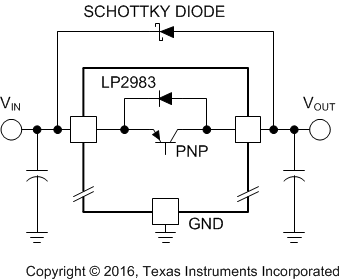
In any application where the output voltage may be higher than the input voltage, an external Schottky diode must be connected from VIN to VOUT (cathode on VIN, anode on VOUT — see Figure 22), to limit the reverse voltage across the LP2983 to 0.3 V (see Absolute Maximum Ratings).
7.3.4 ON/OFF Input Operation
The LP2983 is shut off by driving the ON/OFF input low, and turned on by pulling it high. If this feature is not to be used, the ON/OFF input must be tied to VIN to keep the regulator output on at all times.
To assure proper operation, the signal source used to drive the ON/OFF input must be able to swing above and below the specified turnon or turnoff voltage thresholds listed in Typical Characteristics under VON/OFF. To prevent mis-operation, the turnon (and turnoff) voltage signals applied to the ON/OFF input must have a slew rate which is ≥ 40 mV/µs.
CAUTION
The regulator output voltage can not be ensured if a slow-moving AC (or DC) signal is applied that is in the range between the specified turn-on and turn-off voltages listed under the electrical specification VON/OFF (see Electrical Characteristics).
7.3.5 Thermal Protection
The LP2983 contains a thermal shutdown protection circuit to turn off the output current when excessive heat is dissipated in the LDO. The thermal time-constant of the semiconductor die is fairly short, and thus the output cycles on and off at a high rate when thermal shutdown is reached until the power dissipation is reduced. The internal protection circuitry of the LM2983 is designed to protect against thermal overload conditions. The circuitry is not intended to replace proper heat sinking. Continuously running the device into thermal shutdown degrades its reliability.
7.4 Device Functional Modes
7.4.1 Operation With VO(NOM) + 1 V ≤ VIN < 16 V
The device operates if the input voltage is equal to, or exceeds, VOUT(TARGET) + 1 V. If the previous condition is not met, the device will not operate correctly, and the output voltage may not reach target value.
7.4.2 Operation With ON/OFF Control
If the voltage on the ON/OFF pin is less than 0.1 V at room temperature and less than 0.05 V over the full operating temperature range, the device output is disabled, and the shutdown current (IGND) will not exceed 12 μA. Raising ON/OFF above 1.4 V at room temperature and above 1.6 V over the full operating temperature range initiates the start-up sequence of the device.
