SNVS716H March 2011 – February 2016 LMZ12008
PRODUCTION DATA.
- 1 Features
- 2 Applications
- 3 Description
- 4 Revision History
- 5 Pin Configuration and Functions
- 6 Specification
- 7 Detailed Description
- 8 Application and Implementation
- 9 Power Supply Recommendations
- 10Layout
- 11Device and Documentation Support
- 12Mechanical, Packaging, and Orderable Information
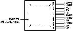
5 Pin Configuration and Functions
NDY Package
11-Pin
Top View

Pin Functions
| PIN | TYPE | DESCRIPTION | |
|---|---|---|---|
| NAME | NO. | ||
| AGND | 3 | Ground | Analog Ground — Reference point for all stated voltages. Must be externally connected to PGND(EP). |
| 5 | |||
| 6 | |||
| EN | 4 | Analog | Enable — Input to the precision enable comparator. Rising threshold is 1.274 V typical. Once the module is enabled, a 13-µA source current is internally activated to facilitate programmable hysteresis. |
| FB | 7 | Analog | Feedback — Internally connected to the regulation amplifier and overvoltage comparator. The regulation reference point is 0.795 V at this input pin. Connect the feedback resistor divider between VOUT and AGND to set the output voltage. |
| NC | 9 | — | No Connect — This pin must remain floating, do not ground. |
| PGND | — | Ground | Exposed Pad / Power Ground — Electrical path for the power circuits within the module. PGND is not internally connected to AGND (pin 5,6). Must be electrically connected to pins 5 and 6 external to the package. The exposed pad is also used to dissipate heat from the package during operation. Use one hundred 12 mil thermal vias from top to bottom copper for best thermal performance. |
| SS | 8 | Analog | Soft-Start/Track Input — To extend the 1.6-ms internal soft-start connect an external soft-start capacitor. For tracking connect to an external resistive divider connected to a higher priority supply rail. See Detailed Design Procedure section. |
| VIN | 1 | Power | Input supply — Nominal operating range is 6 V to 20 V. A small amount of internal capacitance is contained within the package assembly. Additional external input capacitance is required between this pin and the exposed pad (PGND). |
| 2 | |||
| VOUT | 10 | Power | Output Voltage — Output from the internal inductor. Connect the output capacitor between this pin and exposed pad (PGND). |
| 11 | |||