ZHCS568J June   2010  – April 2019 LMZ10505EXT

PRODUCTION DATA.  

  1. 特性
  2. 应用
  3. 说明
    1.     Device Images
      1.      典型应用电路
      2.      效率 (VOUT = 3.3V)
  4. 修订历史记录
  5. Pin Configuration and Functions
    1.     Pin Functions
  6. Specifications
    1. 6.1 Absolute Maximum Ratings
    2. 6.2 ESD Ratings
    3. 6.3 Recommended Operating Conditions
    4. 6.4 Thermal Information
    5. 6.5 Electrical Characteristics
    6. 6.6 Typical Characteristics
  7. Detailed Description
    1. 7.1 Overview
    2. 7.2 Functional Block Diagram
    3. 7.3 Feature Description
      1. 7.3.1 Enable
      2. 7.3.2 Enable and UVLO
      3. 7.3.3 Soft-Start
      4. 7.3.4 Soft-Start Capacitor
      5. 7.3.5 Tracking
      6. 7.3.6 Tracking – Equal Soft-Start Time
      7. 7.3.7 Tracking - Equal Slew Rates
      8. 7.3.8 Current Limit
      9. 7.3.9 Overtemperature Protection
    4. 7.4 Device Functional Modes
      1. 7.4.1 Prebias Start-up Capability
  8. Application and Implementation
    1. 8.1 Application Information
    2. 8.2 Typical Applications
      1. 8.2.1 Design Requirements
      2. 8.2.2 Detailed Design Procedure
        1. 8.2.2.1 Custom Design With WEBENCH® Tools
        2. 8.2.2.2 Input Capacitor Selection
        3. 8.2.2.3 Output Capacitor Selection
          1. 8.2.2.3.1 Output Voltage Setting
        4. 8.2.2.4 Loop Compensation
      3. 8.2.3 Application Curves
        1. 8.2.3.0.1 43
    3. 8.3 System Examples
      1. 8.3.1 Application Schematic for 3.3-V to 5-V Input and 2.5-V Output With Optimized Ripple and Transient Response
      2. 8.3.2 Application Schematic for 3.3-V to 5-V Input and 2.5-V Output
      3. 8.3.3 EMI Tested Schematic for 2.5-V Output Based on 3.3-V to 5-V Input
  9. Power Supply Recommendations
  10. 10Layout
    1. 10.1 Layout Guidelines
    2. 10.2 Layout Examples
    3. 10.3 Estimate Power Dissipation and Thermal Considerations
    4. 10.4 Power Module SMT Guidelines
  11. 11器件和文档支持
    1. 11.1 器件支持
      1. 11.1.1 第三方产品免责声明
      2. 11.1.2 开发支持
        1. 11.1.2.1 使用 WEBENCH® 工具创建定制设计
    2. 11.2 文档支持
      1. 11.2.1 相关文档
    3. 11.3 接收文档更新通知
    4. 11.4 社区资源
    5. 11.5 商标
    6. 11.6 静电放电警告
    7. 11.7 Glossary
  12. 12机械、封装和可订购信息

封装选项

机械数据 (封装 | 引脚)
散热焊盘机械数据 (封装 | 引脚)
订购信息

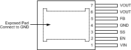
Pin Configuration and Functions

NDW Package
7-Lead TO-PMOD
Top View
LMZ10505EXT 30118372.gif

Pin Functions

PIN TYPE DESCRIPTION
NAME NO.
EN 2 Analog Active-high enable input for the device.
Exposed Pad Ground Exposed pad thermal connection. Connect this pad to the PC board ground plane in order to reduce thermal resistance value. It also provides an electrical connection to the input and output capacitors ground terminals.
FB 5 Analog Feedback pin. This is the inverting input of the error amplifier used for sensing the output voltage.
GND 4 Ground Power ground and signal ground. Connect the bottom feedback resistor between this pin and the feedback pin.
SS 3 Analog Soft-start control pin. An internal 2-uA current source charges and external capacitor connected between this pin and GND (pin 4) to set the output voltage ramp rate during startup. This pin can also be used to configure the tracking feature.
VIN 1 Power A low-ESR input capacitance should be located as close as possible to VIN pin and GND pin.
VOUT 6, 7 Power This is the output of the internal inductor. Connect an external resistor voltage divider from VOUT to FB to ground.