ZHCSDH8 March 2015 LMX2571
PRODUCTION DATA.
- 1 特性
- 2 应用
- 3 说明
- 4 修订历史记录
- 5 Pin Configuration and Functions
- 6 Specifications
-
7 Detailed Description
- 7.1 Overview
- 7.2 Functional Block Diagram
- 7.3
Feature Description
- 7.3.1 Reference Oscillator Input
- 7.3.2 R-Dividers and Multiplier
- 7.3.3 PLL Phase Detector and Charge Pump
- 7.3.4 PLL N-Divider and Fractional Circuitry
- 7.3.5 Partially Integrated Loop Filter
- 7.3.6 Low-Noise, Fully Integrated VCO
- 7.3.7 External VCO Support
- 7.3.8 Programmable RF Output Divider
- 7.3.9 Programmable RF Output Buffer
- 7.3.10 Integrated TX, RX Switch
- 7.3.11 Powerdown
- 7.3.12 Lock Detect
- 7.3.13 FSK Modulation
- 7.3.14 FastLock
- 7.3.15 Register Readback
- 7.4 Device Functional Modes
- 7.5 Programming
- 7.6
Register Maps
- 7.6.1 R60 Register (offset = 3Ch) [reset = 4000h]
- 7.6.2 R58 Register (offset = 3Ah) [reset = C00h]
- 7.6.3 R53 Register (offset = 35h) [reset = 2802h]
- 7.6.4 R47 Register (offset = 2Fh) [reset = 0h]
- 7.6.5 R42 Register (offset = 2Ah) [reset = 210h]
- 7.6.6 R41 Register (offset = 29h) [reset = 810h]
- 7.6.7 R40 Register (offset = 28h) [reset = 101Ch]
- 7.6.8 R39 Register (offset = 27h) [reset = 11F0h]
- 7.6.9 R35 Register (offset = 23h) [reset = 647h]
- 7.6.10 R34 Register (offset = 22h) [reset = 1000h]
- 7.6.11 R33 Register (offset = 21h) [reset = 0h]
- 7.6.12 R25 to R32 Register (offset = 19h to 20h) [reset = 0h]
- 7.6.13 R24 Register (offset = 18h) [reset = 10h]
- 7.6.14 R23 Register (offset = 17h) [reset = 10A4h]
- 7.6.15 R22 Register (offset = 16h) [reset = 8584h]
- 7.6.16 R21 Register (offset = 15h) [reset = 101h]
- 7.6.17 R20 Register (offset = 14h) [reset = 28h]
- 7.6.18 R19 Register (offset = 13h) [reset = 0h]
- 7.6.19 R18 Register (offset = 12h) [reset = 0h]
- 7.6.20 R17 Register (offset = 11h) [reset = 0h]
- 7.6.21 R9 to R16 Register (offset = 9h to 10h) [reset = 0h]
- 7.6.22 R8 Register (offset = 8h) [reset = 10h]
- 7.6.23 R7 Register (offset = 7h) [reset = 10A4h]
- 7.6.24 R6 Register (offset = 6h) [reset = 8584h]
- 7.6.25 R5 Register (offset = 5h) [reset = 101h]
- 7.6.26 R4 Register (offset = 4h) [reset = 28h]
- 7.6.27 R3 Register (offset = 3h) [reset = 0h]
- 7.6.28 R2 Register (offset = 2h) [reset = 0h]
- 7.6.29 R1 Register (offset = 1h) [reset = 0h]
- 7.6.30 R0 Register (offset = 0h) [reset = 3h]
-
8 Application and Implementation
- 8.1
Application Information
- 8.1.1 Direct Digital FSK Modulation
- 8.1.2 Frequency and Output Port Switching with TrCtl Pin
- 8.1.3 OSCin Configuration
- 8.1.4 Register R0 F1F2_INIT, F1F2_MODE usage
- 8.1.5 FastLock with External VCO
- 8.1.6 OSCin Slew Rate
- 8.1.7 RF Output Buffer Power Control
- 8.1.8 RF Output Buffer Type
- 8.1.9 MULT Multiplier
- 8.1.10 Integrated VCO
- 8.2 Typical Applications
- 8.3 Do's and Don'ts
- 8.1
Application Information
- 9 Power Supply Recommendations
- 10Layout
- 11器件和文档支持
- 12机械封装和可订购信息
6 Specifications
6.1 Absolute Maximum Ratings
Over operating free-air temperature range (unless otherwise noted) (1)| MIN | MAX | UNIT | ||
|---|---|---|---|---|
| VCC | Power supply voltage | –0.3 | 3.6 | V |
| VIO | IO supply voltage | –0.3 | 3.6 | V |
| VIN | IO input voltage | VCC + 0.3 | V | |
| VCP | Charge pump supply voltage | 5.25 | V | |
| TJ | Junction temperature | 150 | °C | |
| TSTG | Storage temperature | –65 | 150 | °C |
(1) Stresses beyond those listed under Absolute Maximum Ratings may cause permanent damage to the device. These are stress ratings only, which do not imply functional operation of the device at these or any other conditions beyond those indicated under Recommended Operating Conditions. Exposure to absolute-maximum-rated conditions for extended periods may affect device reliability.
6.2 ESD Ratings
| VALUE | UNIT | |||
|---|---|---|---|---|
| V(ESD) | Electrostatic discharge | Human-body model (HBM), per ANSI/ESDA/JEDEC JS-001(1) | ±1500 | V |
| Charged-device model (CDM), per JEDEC specification JESD22-C101(2) | ±500 | |||
(1) JEDEC document JEP155 states that 500-V HBM allows safe manufacturing with a standard ESD control process.
(2) JEDEC document JEP157 states that 250-V CDM allows safe manufacturing with a standard ESD control process.
6.3 Recommended Operating Conditions
Over operating free-air temperature range (unless otherwise noted)| MIN | MAX | UNIT | |||
|---|---|---|---|---|---|
| VCC | Power supply voltage | 3.15 | 3.45 | V | |
| VIO | IO supply voltage | VCC | V | ||
| VCP | Charge pump supply voltage | PLL mode (external VCO) | 5 | V | |
| Synthesizer mode (internal VCO) | VCC | 5 | |||
| TA | Ambient temperature | –40 | 85 | °C | |
| TJ | Junction Temperature | 125 | °C | ||
6.4 Thermal Information
| THERMAL METRIC(1) | LMX2571 | UNIT | |
|---|---|---|---|
| WQFN (NJK) | |||
| 36 PINS | |||
| RθJA | Junction-to-ambient thermal resistance | 32.9 | °C/W |
| RθJC(top) | Junction-to-case (top) thermal resistance | 14.5 | |
| RθJB | Junction-to-board thermal resistance | 6.3 | |
| ψJT | Junction-to-top characterization parameter | 0.2 | |
| ψJB | Junction-to-board characterization parameter | 6.3 | |
| RθJC(bot) | Junction-to-case (bottom) thermal resistance | 2.0 | |
(1) For more information about traditional and new thermal metrics, see the IC Package Thermal Metrics application report, SPRA953.
6.5 Electrical Characteristics
3.15 V ≤ VCC ≤ 3.45 V, VIO = VCC, –40 °C ≤ TA ≤ 85 °C, except as specified. Typical values are at VCC = VIO = 3.3 V, VCP = 3.3 V or 5 V in synthesizer mode, VCP = 5 V in PLL mode, TA = 25 °C.| PARAMETER | TEST CONDITIONS | MIN | TYP | MAX | UNIT | ||
|---|---|---|---|---|---|---|---|
| CURRENT CONSUMPTION | |||||||
| ICC | Total current in synthesizer mode (internal VCO) | fOUT = 480 MHz SE OSCin |
Configuration A(1) | 39 | mA | ||
| Configuration B(2) | 44 | ||||||
| Configuration C(3) | 46 | ||||||
| Configuration D(4) | 51 | ||||||
| IPLL | Total current in PLL mode (external VCO) | Configuration E(5) | 9 | ||||
| Configuration F(6) | 15 | ||||||
| Configuration G(7) | 21 | ||||||
| ICCPD | Power down current | CE = 0V or POWERDOWN bit = 1 VCC = 3.3 V, Push-pull output |
0.9 | ||||
| OSCIN REFERENCE INPUT | |||||||
| fOSCin | OSCin frequency range | Single-ended or differential input | 10 | 150 | MHz | ||
| VOSCin | OSCin input voltage(8) | Single-ended input | 1.4 | 3.3 | V | ||
| Differential input | 0.15 | 1.5 | |||||
| CRYSTAL REFERENCE INPUT | |||||||
| fXTAL | Crystal frequency range | Fundamental model, ESR < 200 Ω | 10 | 40 | MHz | ||
| CIN | OSCin input capacitance | 1 | pF | ||||
| MULT | |||||||
| fMULTin | MULT input frequency | MULT > Pre-divider Not supported with crystal reference input |
10 | 30 | MHz | ||
| fMULTout | MULT output frequency | 60 | 130 | MHz | |||
| PLL | |||||||
| fPD | Phase detector frequency | 130 | MHz | ||||
| KPD | Charge pump current(9) | Programmable minimum value | Internal charge pump | 312.5 | µA | ||
| 5-V charge pump | 625 | ||||||
| Per programmable step | Internal charge pump | 312.5 | |||||
| 5-V charge pump | 625 | ||||||
| Programmable maximum value | Internal charge pump | 7187.5 | |||||
| 5-V charge pump | 6875 | ||||||
| PNPLL_1/f | Normalized PLL 1/f noise(10) | At maximum charge pump current | Internal charge pump | –124 | dBc/Hz | ||
| 5-V charge pump | –120 | ||||||
| PNPLL_Flat | Normalized PLL noise floor(10) | Internal charge pump | –231 | dBc/Hz | |||
| 5-V charge pump | –226 | ||||||
| fRFin | External VCO input frequency | 100 | 1400 | MHz | |||
| PRFin | External VCO input power | fRFin < 1 GHz | –10 | dBm | |||
| fRFin ≥ 1 GHz | –5 | ||||||
| VCO | |||||||
| fVCO | VCO frequency | 4300 | 5376 | MHz | |||
| KVCO | VCO gain(11) | fVCO = 4800 MHz | 56 | MHz/V | |||
| | ΔTCL | | Allowable temperature drift(12) | VCO not being re-calibrated, –40 °C ≤ TA ≤ 85 °C | 125 | °C | |||
| tVCOCal | VCO calibration time | fOSCin = fPD = 100 MHz | 140 | µs | |||
| PNVCO | Open loop VCO phase noise | fOUT = 480 MHz | 100 Hz offset | –32.4 | dBc/Hz | ||
| 1 kHz offset | –62.3 | ||||||
| 10 kHz offset | –92.1 | ||||||
| 100 kHz offset | –121.1 | ||||||
| 1 MHz offset | –144.5 | ||||||
| 10 MHz offset | –156.8 | ||||||
| RF OUTPUT | |||||||
| fOUT | RF output frequency | Synthesizer mode | 10 | 1344 | MHz | ||
| PLL mode, RF output from buffer | 10 | 1400 | |||||
| PTX, PRX | RF output power | fOUT = 480 MHz | Power control bit = 6 | 0 | dBm | ||
| H2RFout | Second harmonic | –25 | dBc | ||||
| DIGITAL FSK MODULATION | |||||||
| FSKLevel | FSK level(13) | FSK PIN mode | 2 | 8 | |||
| FSKBaud | FSK baud rate(14) | Loop bandwidth = 200 kHz | 100 | kSPs | |||
| FSKDev | FSK deviation | Configuration H(15) | ±39 | kHz | |||
| DIGITAL INTERFACE | |||||||
| VIH | High level input voltage | 1.4 | VIO | V | |||
| VIL | Low level input voltage | 0.4 | V | ||||
| IIH | High level input current | VIH = 1.75 V | –25 | 25 | µA | ||
| IIL | Low level input current | VIL = 0 V | –25 | 25 | µA | ||
| VOH | High level output voltage | IOH = 500 µA | 2 | V | |||
| VOL | Low level output voltage | IOL = –500 µA | 0 | 0.4 | V | ||
(1) fOSCin = 19.44 MHz, MULT = 1, Prescaler = 4, fPD = 19.44 MHz, one RF output, output type = push pull, output power = –3 dBm
(2) fOSCin = 19.44 MHz, MULT = 1, Prescaler = 2, fPD = 19.44 MHz, one RF output, output type = push pull, output power = –3 dBm
(3) fOSCin = 19.44 MHz, MULT = 5, Prescaler = 2, fPD = 19.44 MHz, one RF output, output type = push pull, output power = –3 dBm
(4) fOSCin = 19.44 MHz, MULT = 5, Prescaler = 2, fPD = 97.2 MHz, one RF output, output type = push pull, output power = –3 dBm
(5) fOSCin = 19.44 MHz, MULT = 1, fPD = 19.44 MHz, output from VCO
(6) fOSCin = 19.44 MHz, MULT = 1, fPD = 19.44 MHz, one RF output, output type = push pull, output power = –3 dBm
(7) fOSCin = 19.44 MHz, MULT = 1, fPD = 19.44 MHz, two RF outputs, output type = push pull, output power = –3 dBm
(8) See OSCin Configuration for definition of OSCin input voltage.
(9) This is referring to the total base charge pump current. In PLL mode, this is equal to EXTVCO_CP_IDN + EXTVCO_CP_IUP. In synthesizer mode, this is equal to CP_IDN + CP_IUP. See Table 5, Table 6 and Table 7 for details.
(10) Measured with a clean OSCin signal with a high slew rate using a wide loop bandwidth. The noise metrics model the PLL noise for an infinite loop bandwidth as:
PLL_Total = 10 * log[10(PLL_Flat / 10) + 10(PLL_Flicker / 10)]
PLL_Flat = PN1Hz + 20 * log(N) + 10 * log(fPD)
PLL_Flicker = PN10kHz – 10 * log(Offset / 10 kHz) + 20 * log(fOUT / 1 GHz)
PLL_Total = 10 * log[10(PLL_Flat / 10) + 10(PLL_Flicker / 10)]
PLL_Flat = PN1Hz + 20 * log(N) + 10 * log(fPD)
PLL_Flicker = PN10kHz – 10 * log(Offset / 10 kHz) + 20 * log(fOUT / 1 GHz)
(11) The VCO gain changes as a function of the VCO core and frequency. See Integrated VCO for details.
(12) Not tested in production. Ensured by characterization. Allowable temperature drift refers to programming the device at an initial temperature and allowing this temperature to drift WITHOUT reprogramming the device, and still have the device stay in lock. This change could be up or down in temperature and the specification does not apply to temperatures that go outside the recommended operating temperatures of the device.
(13) The data showed here simply specifies the range of discrete FSK level that is supported in PIN mode. PIN mode supports 2-, 4- and 8-level of FSK modulation. If arbitrary level of FSK modulation is desired, use FSK SPI™ FAST mode or FSK I2S mode. See Direct Digital FSK Modulation for details.
(14) The baud rate is limited by the loop bandwidth of the PLL loop. As a general rule of thumb, it is desirable to have the loop bandwidth at least twice the baud rate.
(15) fPD = 100 MHz, DEN = 224, CHDIV1 = 5, CHDIV2 = 2, Prescaler = 2, FSK step value = 32716, 32819. The maximum achievable frequency deviation depends on the configuration, see Direct Digital FSK Modulation for details.
6.6 Timing Requirements
3.15 V ≤ VCC ≤ 3.45 V, VIO = VCC, –40 °C ≤ TA ≤ 85 °C, except as specified. Typical values are at VCC = VIO = 3.3 V, TA = 25 °C.| MIN | NOM | MAX | UNIT | |||
|---|---|---|---|---|---|---|
| MICROWIRE TIMING | ||||||
| tES | Clock to enable low time | See Figure 1 | 5 | ns | ||
| tCS | Data to clock setup time | 2 | ns | |||
| tCH | Data to clock hold time | 2 | ns | |||
| tCWH | Clock pulse width high | 5 | ns | |||
| tCWL | Clock pulse width low | 5 | ns | |||
| tCES | Enable to clock setup time | 5 | ns | |||
| tEWH | Enable pulse width high | 2 | ns | |||
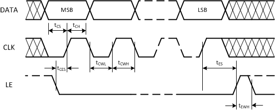 Figure 1. MICROWIRE Timing Diagram
There are several other considerations for programming:
- A slew rate of at least 30 V/µs is recommended for the CLK, DATA and LE. The same apply for other digital control signals such as FSK_D[0:2] and FSK_DV signals.
- The DATA is clocked into a shift register on each rising edge of the CLK signal. On the rising edge of the LE signal, the data is sent from the shift register to an active register.
- The LE pin may be held high after programming, causing the LMX2571 to ignore clock pulses.
- When CLK or DATA lines are shared between devices, it is recommended to divide down the voltage to the CLK, DATA, and LE pins closer to the minimum voltage. This provides better noise immunity.
- If the CLK and DATA lines are toggled while the VCO is in lock, as is sometimes the case when these lines are shared with other parts, the phase noise may be degraded during the time of this programming.
6.7 Typical Characteristics
At TA = 25 °C, unless otherwise noted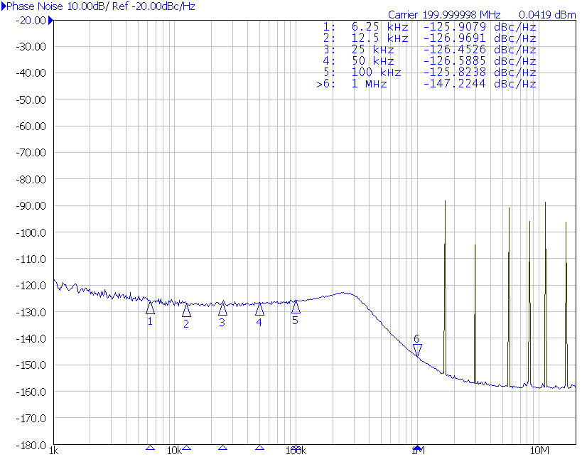
| OSCin = 19.44 MHz | fOUT = 200 MHz | Synthesizer mode |
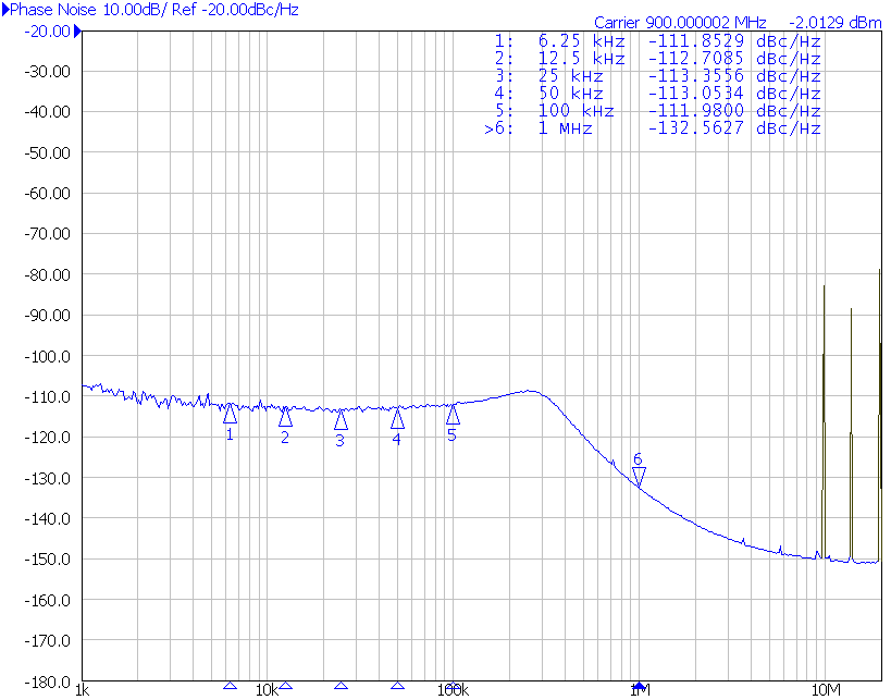
| OSCin = 19.44 MHz | fOUT = 900 MHz | Synthesizer mode |
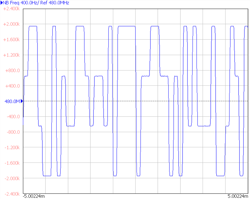
| FSKBaud = 4.8 kSPS | FSK PIN mode |
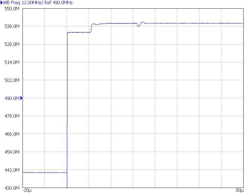
| Switching between int. and ext. VCO as well as Tx and Rx port |
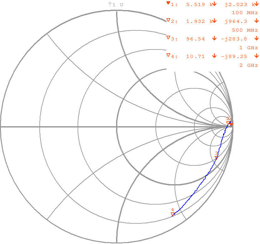
| Start: 100 MHz | Stop: 2000 MHz |
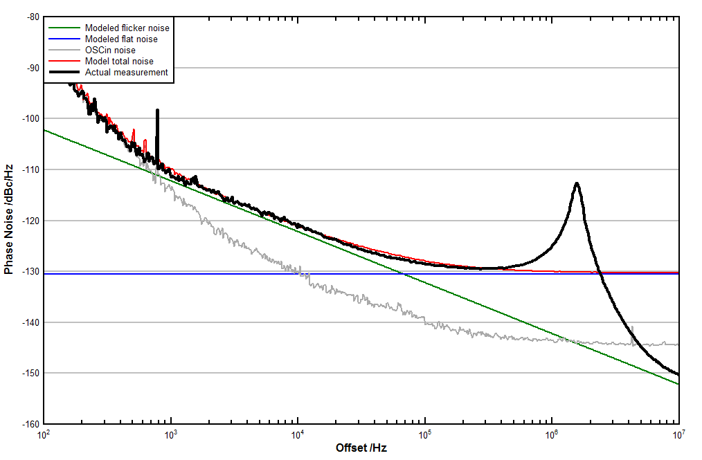
| fOUT = 1228.8 MHz | fPD = 122.88 MHz | Synthesizer mode |
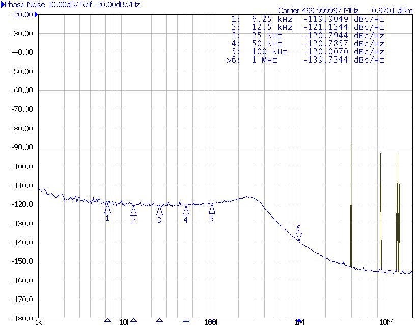
| OSCin = 19.44 MHz | fOUT = 500 MHz | Synthesizer mode |
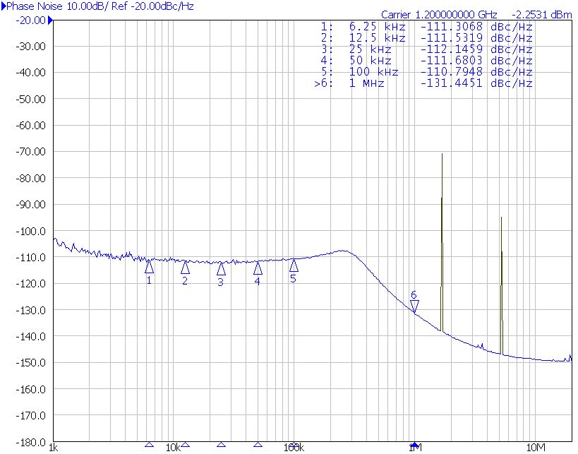
| OSCin = 19.44 MHz | fOUT = 1200 MHz | Synthesizer mode |
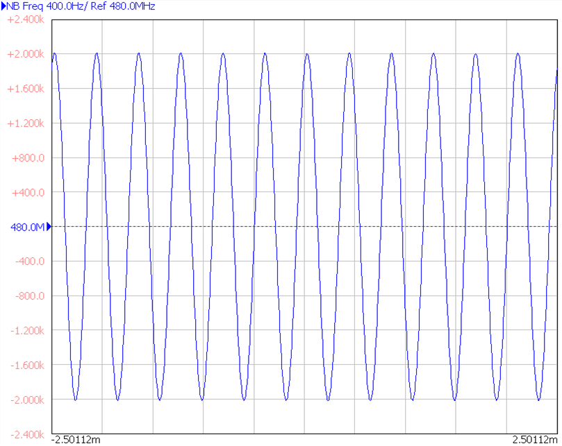
| Reference clock is a FM modulated signal with fMOD = 2.4 kHz |
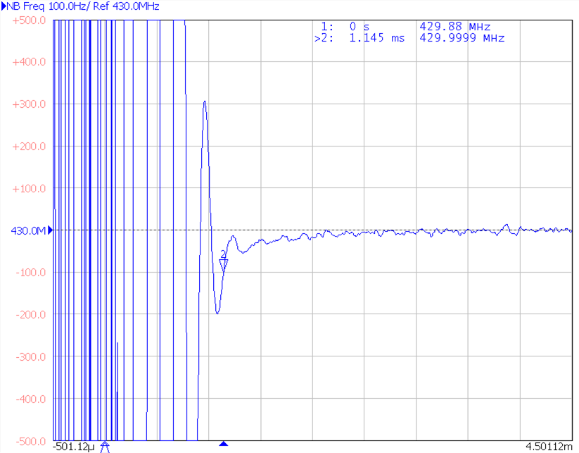
| Freq. jump = 50 MHz | LBW = 4 kHz | PLL mode |
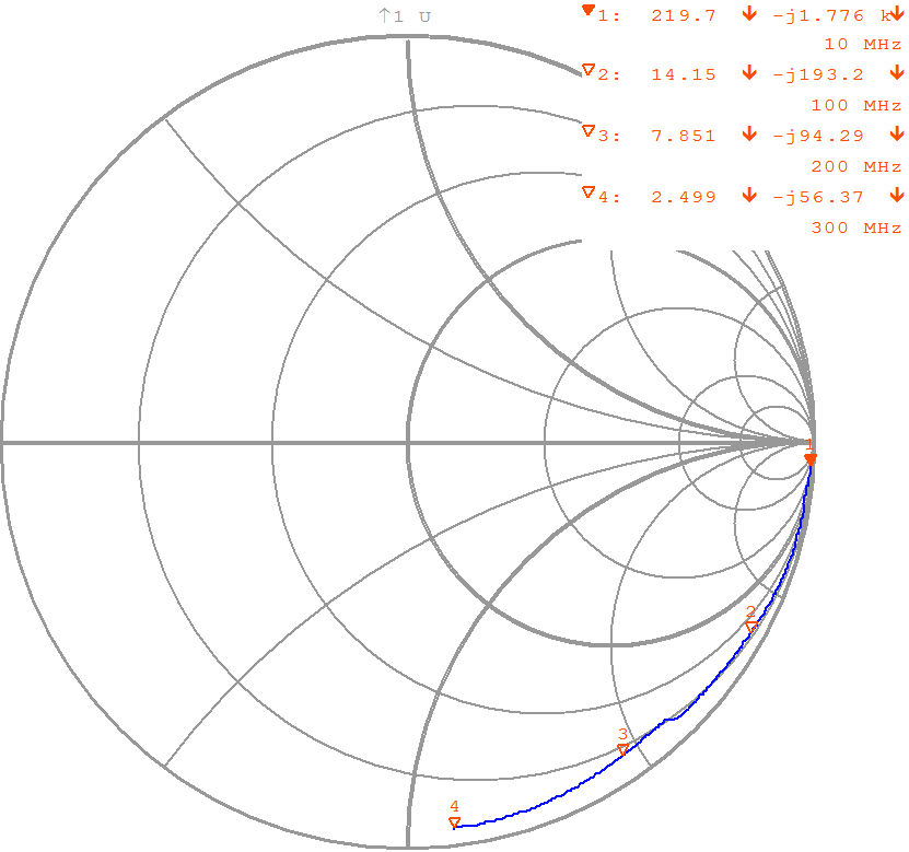
| Start: 10 MHz | Stop: 300 MHz |
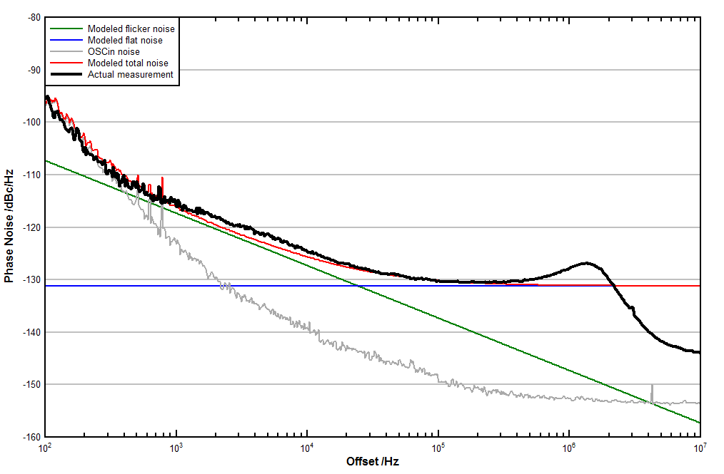
| fOUT = 430.08 MHz | fPD = 61.44 MHz | PLL mode |