SNAS324B January   2006  – January 2016 LMX2486

PRODUCTION DATA.  

  1. Features
  2. Applications
  3. Description
  4. Revision History
  5. Pin Configuration and Functions
  6. Specifications
    1. 6.1 Absolute Maximum Ratings
    2. 6.2 ESD Ratings
    3. 6.3 Recommended Operating Conditions
    4. 6.4 Thermal Information
    5. 6.5 Electrical Characteristics
    6. 6.6 Timing Requirements
    7. 6.7 Typical Characteristics
      1. 6.7.1 Sensitivity
      2. 6.7.2 FinRF Input Impedance
      3. 6.7.3 FinIF Input Impedance
      4. 6.7.4 OSCin Input Impedance
      5. 6.7.5 Currents
  7. Parameter Measurements Information
    1. 7.1 Bench Test Set-Ups
      1. 7.1.1 Charge Pump Current Measurement
      2. 7.1.2 Charge Pump Current Specification Definitions
        1. 7.1.2.1 Charge Pump Output Current Variation vs Charge Pump Output Voltage
        2. 7.1.2.2 Charge Pump Output Current Variation vs Temperature
      3. 7.1.3 Sensitivity Measurement
      4. 7.1.4 Input Impedance Measurement
  8. Detailed Description
    1. 8.1 Overview
    2. 8.2 Functional Block Diagram
    3. 8.3 Feature Description
      1. 8.3.1 TCXO, Oscillator Buffer, and R Counter
      2. 8.3.2 Phase Detector
      3. 8.3.3 Charge Pump
      4. 8.3.4 Loop Filter
      5. 8.3.5 N Counters and High Frequency Input Pins
        1. 8.3.5.1 High Frequency Input Pins, FinRF and FinIF
        2. 8.3.5.2 Complementary High Frequency Pin, FinRF*
      6. 8.3.6 Digital Lock Detect Operation
      7. 8.3.7 Cycle Slip Reduction and Fastlock
        1. 8.3.7.1 Cycle Slip Reduction (CSR)
        2. 8.3.7.2 Fastlock
        3. 8.3.7.3 Using Cycle Slip Reduction (CSR) to Avoid Cycle Slipping
        4. 8.3.7.4 Using Fastlock to Improve Lock Times
        5. 8.3.7.5 Capacitor Dielectric Considerations for Lock Time
      8. 8.3.8 Fractional Spur and Phase Noise Controls
    4. 8.4 Device Functional Modes
      1. 8.4.1 Power Pins, Power-Down, and Power-Up Modes
    5. 8.5 Programming
      1. 8.5.1 General Programming Information
        1. 8.5.1.1 Register Location Truth Table
        2. 8.5.1.2 Control Register Content Map
    6. 8.6 Register Maps
      1. 8.6.1 R0 Register
        1. 8.6.1.1 RF_FN[11:0] -- Fractional Numerator for RF PLL
        2. 8.6.1.2 RF_N[10:0] -- RF N Counter Value
      2. 8.6.2 R1 Register
        1. 8.6.2.1 RF_FD[11:0] -- RF PLL Fractional Denominator
        2. 8.6.2.2 RF_R [5:0] -- RF R Divider Value
        3. 8.6.2.3 RF_P -- RF Prescaler bit
        4. 8.6.2.4 RF_PD -- RF Power Down Control Bit
      3. 8.6.3 R2 Register
        1. 8.6.3.1 IF_N[18:0] -- IF N Divider Value
        2. 8.6.3.2 IF_PD -- IF Power Down Bit
      4. 8.6.4 R3 Register
        1. 8.6.4.1 IF_R[11:0] -- IF R Divider Value
        2. 8.6.4.2 RF_CPG -- RF PLL Charge Pump Gain
        3. 8.6.4.3 Access -- Register Access Word
      5. 8.6.5 R4 Register
        1. 8.6.5.1 MUX[3:0] Frequency Out and Lock Detect MUX
        2. 8.6.5.2 IF_P -- IF Prescaler
        3. 8.6.5.3 RF_CPP -- RF PLL Charge Pump Polarity
        4. 8.6.5.4 IF_CPP -- IF PLL Charge Pump Polarity
        5. 8.6.5.5 OSC_OUT Oscillator Output Buffer Enable
        6. 8.6.5.6 OSC2X -- Oscillator Doubler Enable
        7. 8.6.5.7 FM[1:0] -- Fractional Mode
        8. 8.6.5.8 DITH[1:0] -- Dithering Control
        9. 8.6.5.9 ATPU -- PLL Automatic Power Up
      6. 8.6.6 R5 Register
        1. 8.6.6.1 Fractional Numerator Determination { RF_FN[21:12], RF_FN[11:0], Access[1] }
        2. 8.6.6.2 Fractional Denominator Determination { RF_FD[21:12], RF_FD[11:0], Access[1]}
      7. 8.6.7 R6 Register
        1. 8.6.7.1 RF_TOC -- RF Time-Out Counter and Control for FLoutRF Pin
        2. 8.6.7.2 RF_CPF -- RF PLL Fastlock Charge Pump Current
        3. 8.6.7.3 CSR[1:0] -- RF Cycle Slip Reduction
      8. 8.6.8 R7 Register
        1. 8.6.8.1 DIV4 -- RF Digital Lock Detect Divide By 4
        2. 8.6.8.2 IF_RST -- IF PLL Counter Reset
        3. 8.6.8.3 RF_RST -- RF PLL Counter Reset
        4. 8.6.8.4 RF_TRI -- RF Charge Pump TRI-STATE
        5. 8.6.8.5 IF_TRI -- IF Charge Pump TRI-STATE
  9. Application and Implementation
    1. 9.1 Application Information
    2. 9.2 Typical Application
      1. 9.2.1 Design Requirements
      2. 9.2.2 Detailed Design Procedure
      3. 9.2.3 Application Curves
  10. 10Power Supply Recommendations
  11. 11Layout
    1. 11.1 Layout Guidelines
    2. 11.2 Layout Example
  12. 12Device and Documentation Support
    1. 12.1 Community Resources
    2. 12.2 Trademarks
    3. 12.3 Electrostatic Discharge Caution
    4. 12.4 Glossary
  13. 13Mechanical, Packaging, and Orderable Information

封装选项

机械数据 (封装 | 引脚)
散热焊盘机械数据 (封装 | 引脚)
订购信息

11 Layout

11.1 Layout Guidelines

The critical pin is the high freqeuncy input pin that should have a short trace. In general, try to keep the ground and power planes 20 mils or more farther away from vias to supply pins to ensure that no spur energy can couple to them.

11.2 Layout Example
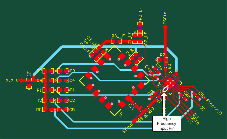
LMX2486 pcb_snas324.gif Figure 27. Simplified Layout for Only RF PLL Used