SNAS187D February 2003 – January 2016 LMX2430 , LMX2433 , LMX2434
PRODUCTION DATA.
- 1 Features
- 2 Applications
- 3 Description
- 4 Revision History
- 5 Description continued
- 6 Pin Configuration and Functions
- 7 Specifications
- 8 Parameter Measurement Information
-
9 Detailed Description
- 9.1 Overview
- 9.2 Functional Block Diagram
- 9.3 Feature Description
- 9.4 Device Functional Modes
- 9.5 Programming
- 9.6
Register Maps
- 9.6.1 Control Register Content Map
- 9.6.2
R0 Register
- 9.6.2.1 RF_R[14:0] - RF Synthesizer Programmable Reference Divider (R Counter) (R0[17:3])
- 9.6.2.2 RF_CPP - RF Synthesizer Phase Detector Polarity (R0[18])
- 9.6.2.3 RF_CPG - RF Synthesizer Charge-Pump Current Gain (R0[19])
- 9.6.2.4 RF_CPT - RF Synthesizer Charge-Pump Tri-State (R0[20])
- 9.6.2.5 RF_RST - RF Synthesizer Counter Reset (R0[21])
- 9.6.3 R1 Register
- 9.6.4
R2 Register
- 9.6.4.1 RF_TOC[0:11] - RF Synthesizer Time-Out Counter (R2[14:3])
- 9.6.4.2
R3 Register
- 9.6.4.2.1 IF_R[14:0] - IF Synthesizer Programmable Reference Divider (R Counter) (R3[17:3])
- 9.6.4.2.2 IF_CPP - IF Synthesizer Phase Detector Polarity (R3[18])
- 9.6.4.2.3 IF_CPG - IF Synthesizer Charge-Pump Current Gain (R3[19])
- 9.6.4.2.4 IF_CPT - IF Synthesizer Charge-Pump Tri-State (R3[20])
- 9.6.4.2.5 IF_RST - IF Synthesizer Counter Reset (R3[21])
- 9.6.5 R4 Register
- 9.6.6 R5 Register
- 9.6.7 MUX[3:0] - Multifunction Output Select (R3[23:22]:R0[23:22])
- 10Application and Implementation
- 11Power Supply Recommendations
- 12Layout
- 13Device and Documentation Support
- 14Mechanical, Packaging, and Orderable Information
8 Parameter Measurement Information
8.1 Bench Test Setups
8.1.1 LMX243x Charge-Pump Test Setup
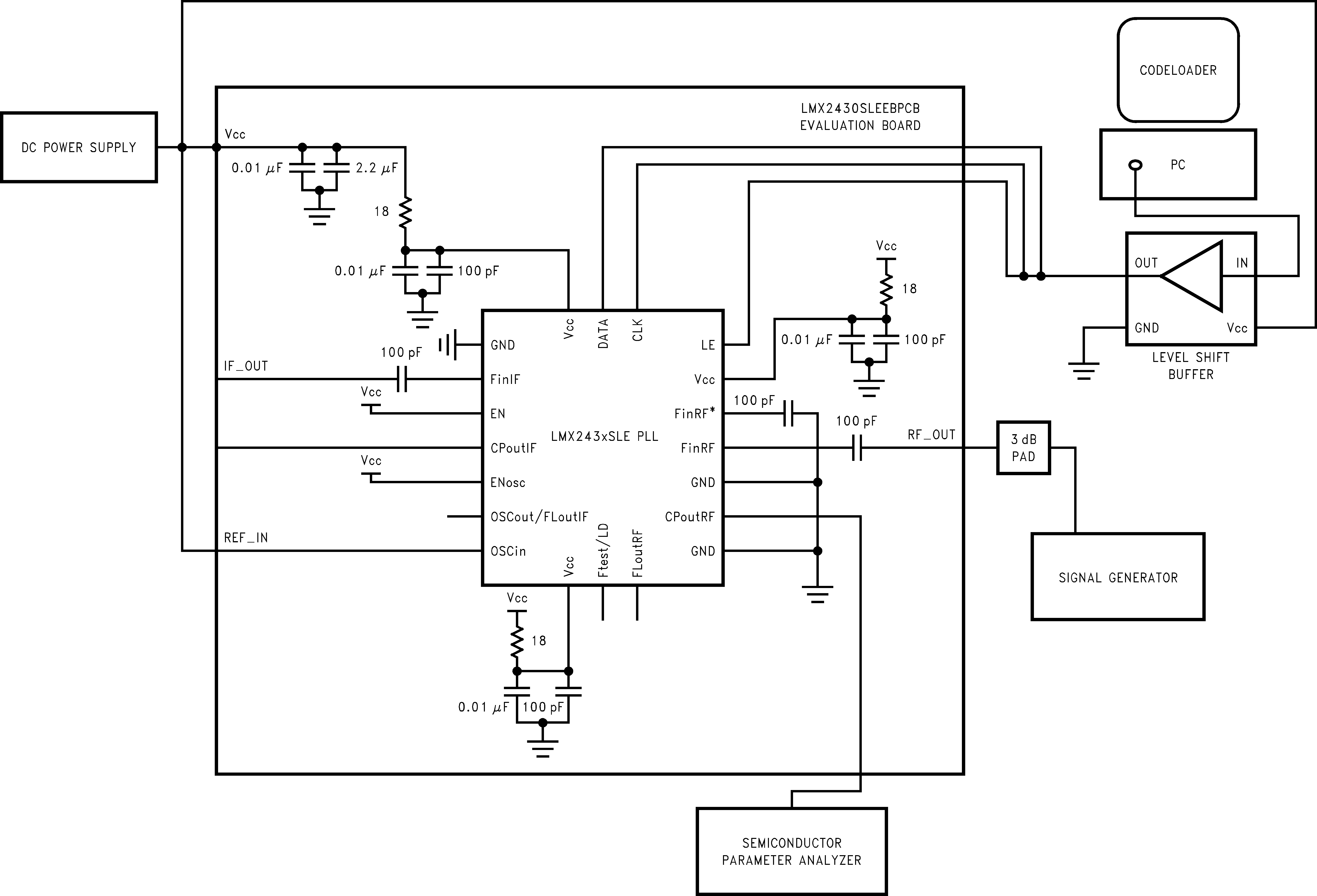 Figure 23. Charge-Pump Current Test Setup
Figure 23 shows the setup required to measure the RF charge-pump sink current of the LMX243x device. The same setup is used for the LMX2430PW evaluation board. The purpose of this test is to assess the functionality of the RF charge pump. The IF charge pump is evaluated in the same way.
This setup uses an open-loop configuration. A power supply is connected to VCC. By means of a signal generator, a 10-MHz signal is typically applied to the FinRF pin. The signal is one of two inputs to the phase / frequency detector (PFD). The 3-dB pad provides a 50-Ω match between the PLL and the signal generator. The OSCin pin is tied to Vcc. This establishes the other input to the PFD. Alternatively, this input can be tied directly to the ground plane. The EN and ENosc pins are also both tied to Vcc. A semiconductor parameter analyzer is connected to the CPoutRF pin and used to measure the sink, source, and tri-state leakage currents.
Let Fr represent the frequency of the signal applied to the OSCin pin, which is simply zero in this case (DC), and let Fp represent the frequency of the signal applied to the FinRF pin. The PFD is sensitive to the rising edges of Fr and Fp. Assuming positive VCO characteristics (RF_CPP bit = 1); the charge pump turns ON, and sinks current when the first rising edge of Fp is detected. Because Fr has no rising edge, the charge pump continues to sink current indefinitely. In order to measure the RF charge-pump source current, the RF_CPP bit is simply set to 0 (negative VCO characteristics) in CodeLoader. Similarly, in order to measure the tri-state leakage current, the RF_CPT bit is set to 1.
The measurements are typically taken over supply voltage and temperature. The measurements are also typically taken at the HIGH and LOW charge-pump current gains. The charge-pump current gain can be controlled by the RF_CPG bit in CodeLoader. Once the charge-pump currents are determined, the (i) charge-pump output current magnitude variation versus charge-pump output voltage, (ii) charge-pump output sink current versus charge-pump output source current mismatch, and (iii) charge-pump output current magnitude versus temperature, can be calculated. Refer to the Charge Pump Current Specifications Definition for more details.
8.1.2 Charge-Pump Current Specification Definitions
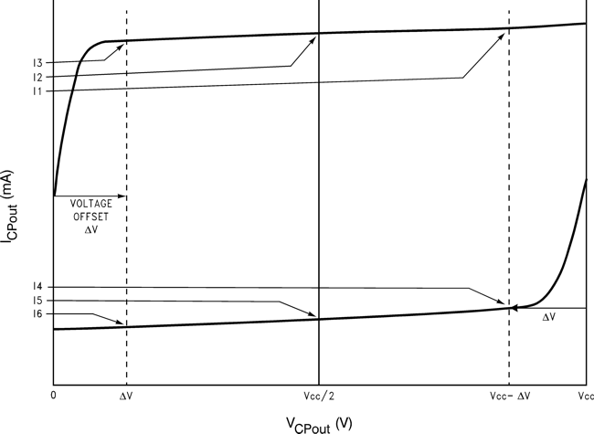
I2 = Charge-Pump Sink Current at VCPout = Vcc//2
I3 = Charge-Pump Sink Current at VCPout = ΔV
I4 = Charge-Pump Source Current at VCPout = Vcc − ΔV
I5 = Charge-Pump Source Current at VCPout = Vcc/2
I6 = Charge-Pump Source Current at VCPout = ΔV
ΔV = Voltage offset from the positive and negative rails. Dependent on the VCO tuning range relative to Vcc and GND. Typical values are between 0.5V and 1.0V.
VCPout refers to either VCPoutRF or VCPoutIF
ICPout refers to either ICPoutRF or ICPoutIF
8.1.2.1 Charge-Pump Output Current Variation vs Charge-Pump Output Voltage
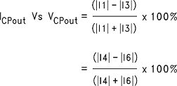
8.1.2.2 Charge-Pump Sink Current vs Charge-Pump Output Source Current Mismatch

8.1.2.3 Charge-Pump Output Current Variation vs Temperature

8.1.3 LMX243x FinRF Sensitivity Test Setup
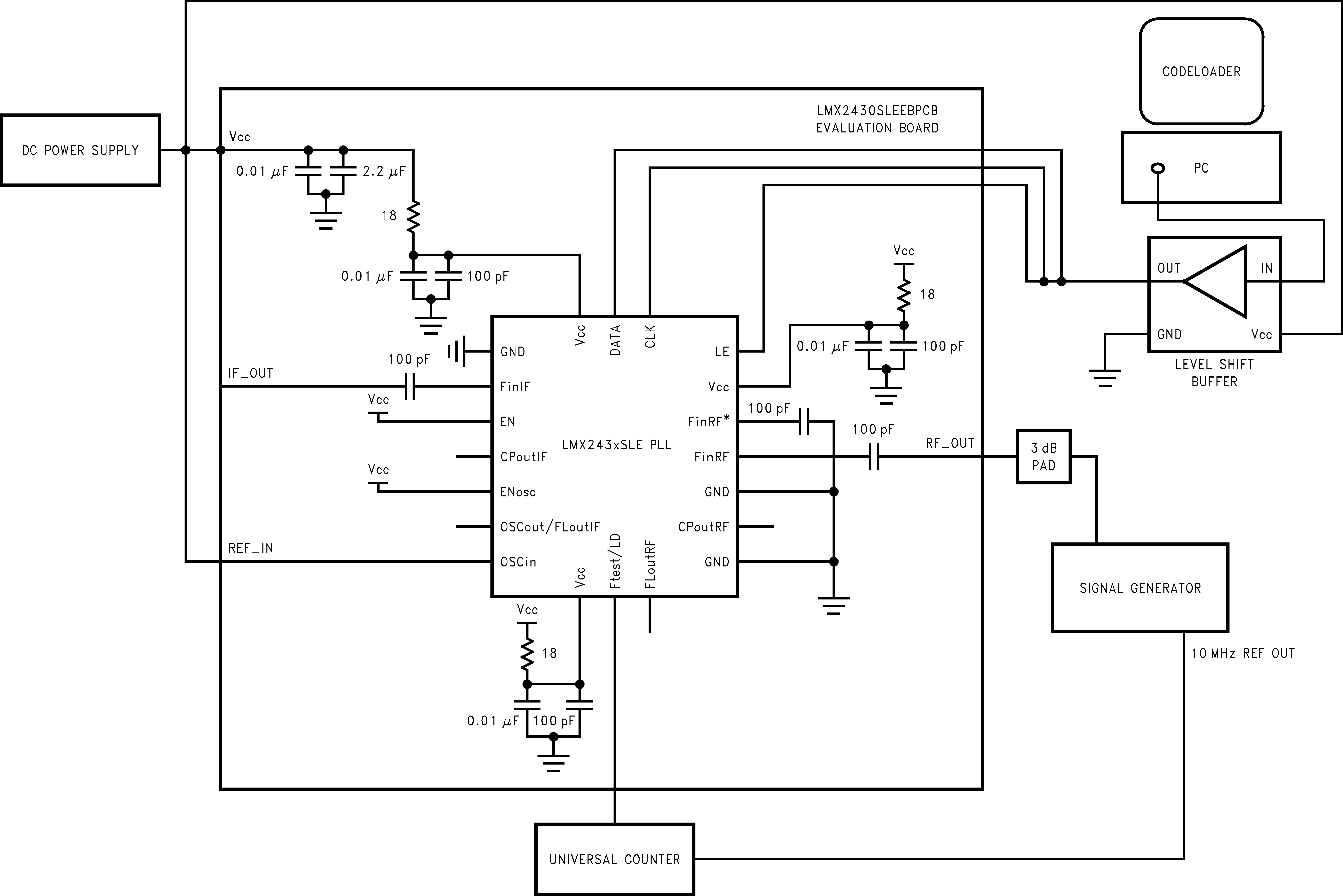 Figure 25. RF Input Sensitivity Test Setup
Figure 25 shows the setup required to measure the RF input sensitivity level of the LMX243x device. The same setup is used for the LMX2430PW evaluation board. The purpose of this test is to measure the acceptable signal level to the FinRF input of the PLL chip. Outside the acceptable signal range, the feedback divider begins to divide incorrectly and miscount the frequency. The FinIF sensitivity is evaluated in the same way.
The setup uses an open-loop configuration. A power supply is connected to Vcc. The IF PLL is powered down (IF_PD bit = 1). By means of a signal generator, an RF signal is applied to the FinRF pin. The 3-dB pad provides a 50-Ω match between the PLL and the signal generator. The EN, ENosc, and OSCin pins are all tied to VCC. The N value is typically set to 10000 in CodeLoader, that is, RF_B word = 156 and RF_A word = 16 for RF_P bit = 0 (LMX2434) or RF_P bit = 1 (LMX2430 and LMX2433). The feedback divider output is routed to the Ftest/LD pin by selecting the RF_N/2 Frequency word (MUX[3:0] word = 15) in CodeLoader. A Universal Counter is connected to the Ftest/LD pin and used to monitor the output frequency of the feedback divider. The expected frequency must be the signal generator frequency divided by twice the corresponding counter value, that is, 20,000. The factor of two comes in because the LMX43x device has an internal /2 circuit which is used to provide a 50% duty cycle.
Sensitivity is typically measured over frequency, supply voltage and temperature. In order to perform the measurement, the temperature, frequency, and supply voltage is set to a fixed value, and the power level of the signal at FinRF is varied. Sensitivity is reached when the frequency error of the divided RF input is greater than or equal to 1 Hz. The power attenuation from the cable and the 3-dB pad must be accounted for. The feedback divider miscounts if too much or too little power is applied to the FinRF input. Therefore, the allowed input power level is bounded by the upper and lower sensitivity limits. In a typical application, if the power level to the FinRF input approaches the sensitivity limits, this can introduce spurs or cause degradation to the phase noise. When the power level gets even closer to these limits, or exceeds them, the RF PLL loses lock.
8.1.4 LMX243x OSCin Sensitivity Test Setup
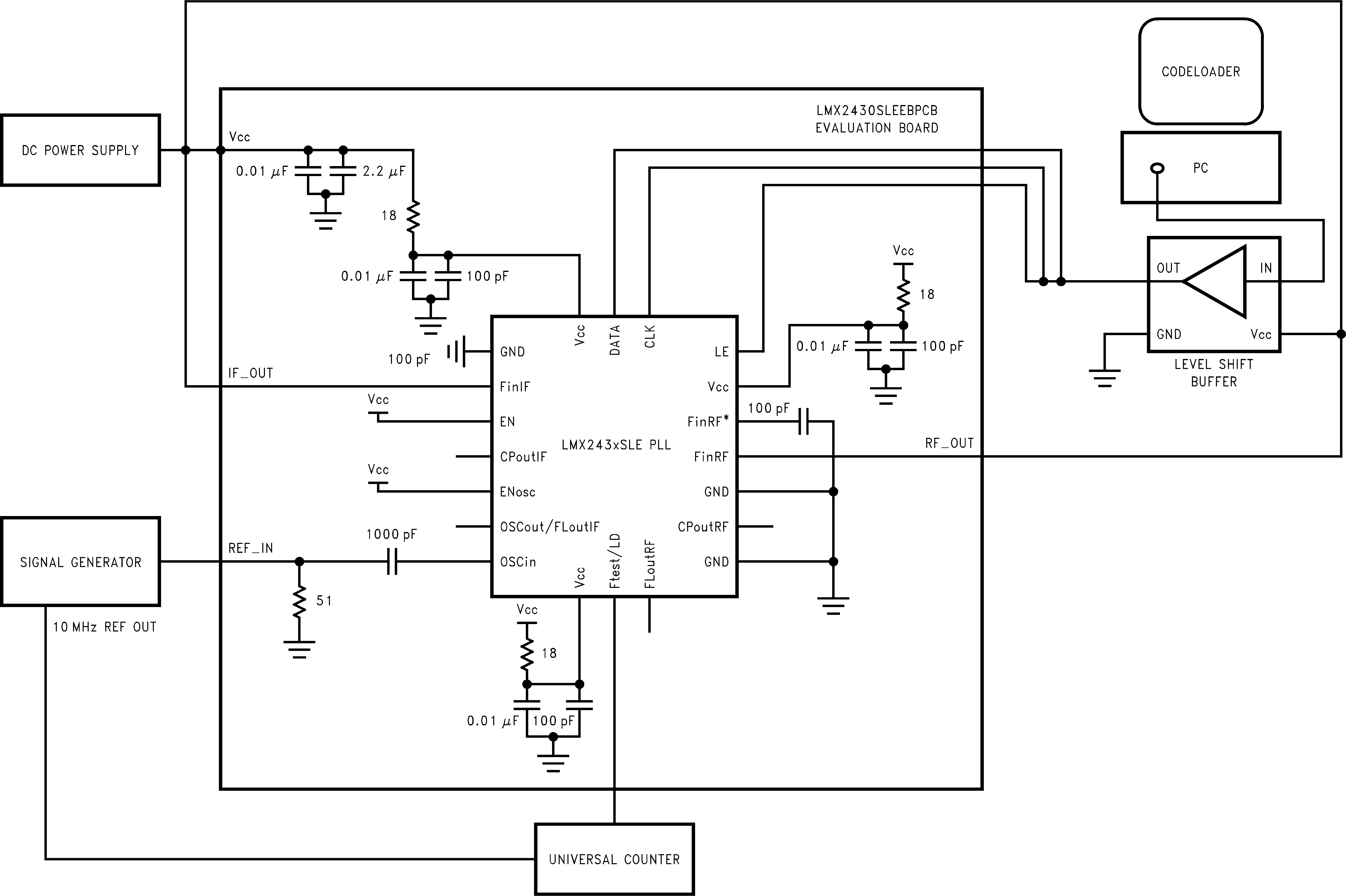 Figure 26. OSCin Sensitivity Test Setup
Figure 26 shows the setup required to measure the OSCin buffer sensitivity level in the LMX243x device. The same setup is used for the LMX2430PW evaluation board. This setup is similar to the FinRF sensitivity setup except that the signal generator is now connected to the OSCin pin, and both Fin pins are tied to VCC. The 51-Ω shunt resistor matches the OSCin input to the signal generator. The R counter is typically set to 1000, that is, RF_R word = 1000 or IF_R word = 1000. The reference divider output is routed to the Ftest/LD pin by selecting the RF_R/ 2 frequency word (MUX[3:0] word = 14) or the IF_R/ 2 frequency word (MUX[3:0] word = 12) in CodeLoader. A universal counter is connected to the Ftest/LD pin and is used to monitor the output frequency of the reference divider. The expected frequency must be the signal generator frequency divided by twice the corresponding counter value, that is, 2000. The factor of two comes in because the LMX243x device has an internal /2 circuit which is used to provide a 50% duty cycle.
In a similar way, sensitivity is typically measured over frequency, supply voltage and temperature. In order to perform the measurement, the temperature, frequency, and supply voltage is set to a fixed value and the power level (voltage level) of the signal at OSCin is varied. Sensitivity is reached when the frequency error of the divided input signal is greater than or equal to 1 Hz.
8.1.5 LMX243x FinRF Input Impedance Test Setup
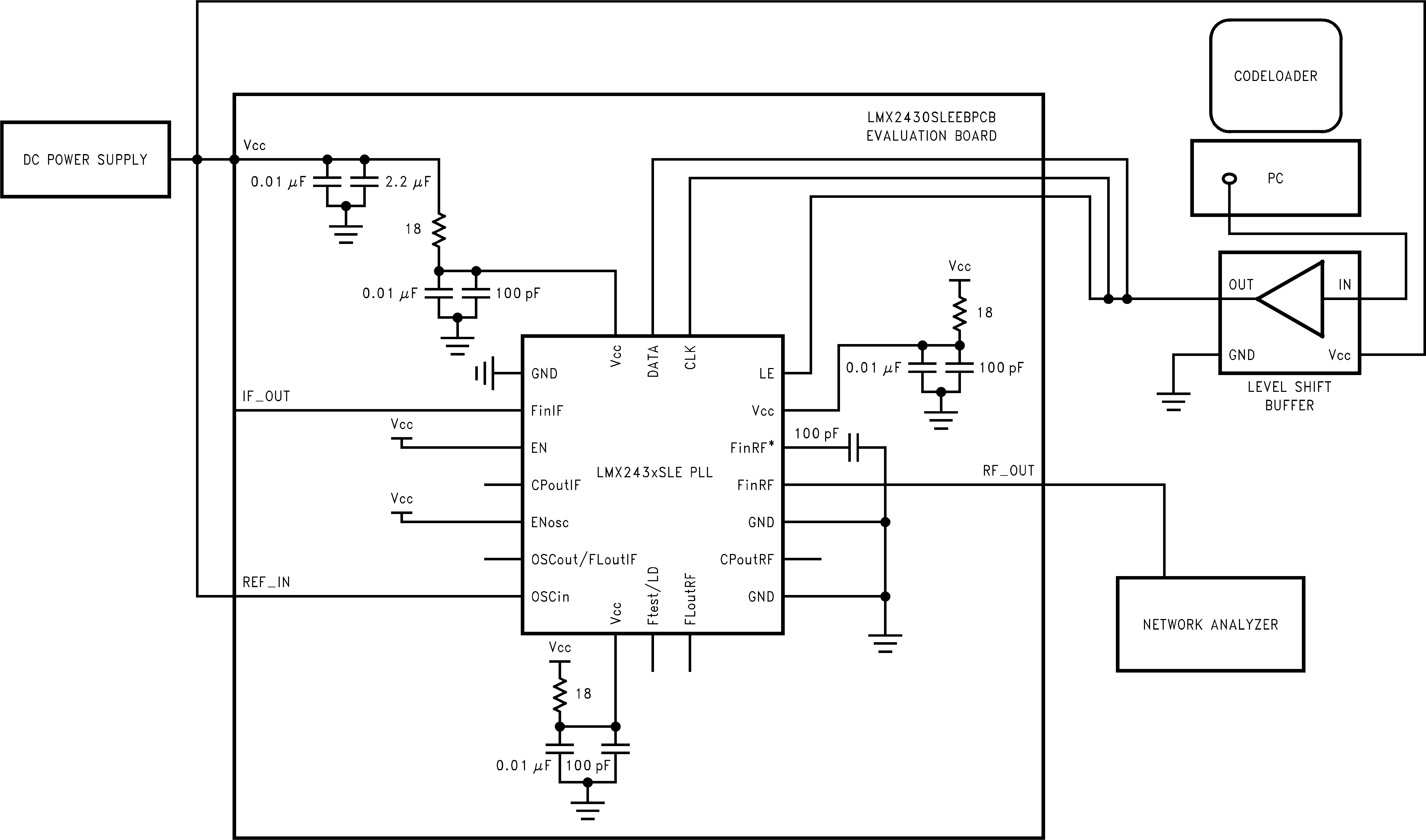 Figure 27. Imput Impedance Test Setup
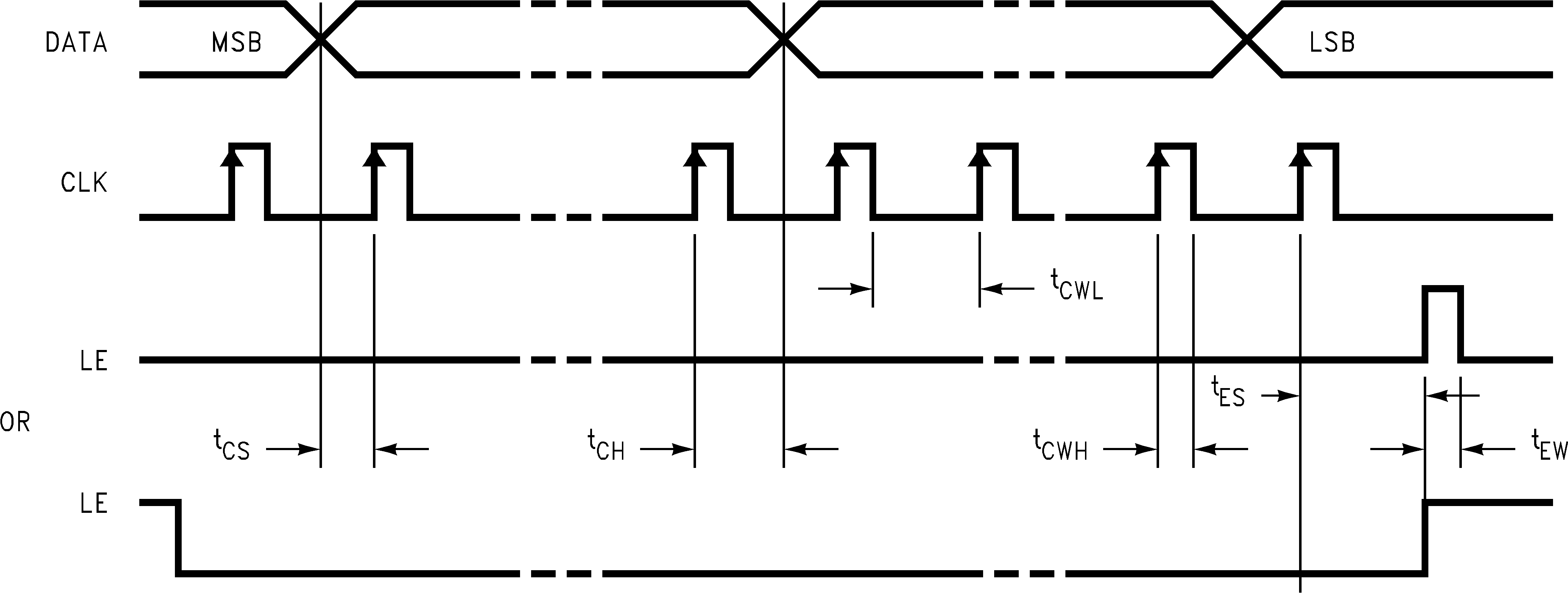
1. DATA is clocked into the 24-bit shift register on the rising edge of CLK
2. The MSB of DATA is shifted in first.
Figure 28 shows the setup required to measure the RF input impedance of the LMX243x device. The same setup is used for the LMX2430PW evaluation board. Measuring the input impedance of the device facilitates the design of appropriate matching networks to match the PLL to the VCO, or in more critical situations, to the characteristic impedance of the printed-circuit-board (PCB) trace, to prevent undesired transmission line effects. The FinIF input impedance is evaluated in the same way.
Before the actual measurements are taken, the network analyzer must be calibrated, that is, the error coefficients must be calculated. The calibration standard of the network analyzer is used to calculate these coefficients. The calibration standard includes an open, short and a matched load. A 1-port calibration is implemented here.
To calculate the coefficients, the PLL chip is first removed from the PCB. A piece of semi-rigid coaxial cable is then soldered to the pad on the PCB which is equivalent to the FinRF pin on the PLL chip. Proper grounding near the exposed tip of the semi-rigid coaxial cable is required for accurate results. The DC blocking capacitor is removed for this test. The network analyzer port is then connected to the other end of the semi-rigid coaxial cable. In this way, the semi-rigid coaxial cable acts as a transmission line. This transmission line adds electrical length and produces an offset from the reference plane of the network analyzer; therefore, it must be included in the calibration. The desired operating frequency is then set. The typical frequency range selected for the RF synthesizer of the LMX243x device is from 100 MHz to 6000 MHz.
The network analyzer calculates the calibration coefficients based on the measured S11 parameters. With this all done, calibration is now complete.
The PLL chip is then placed on the PCB, and a power supply connected to VCC. The EN, ENosc, and OSCin pins are all tied to VCC. Alternatively, the OSCin pin can be tied to ground. In this setup, the complementary input (FinRF*) is AC-coupled to ground. With the network analyzer still connected to the semi-rigid coaxial cable, the measured FinRF impedance is displayed.
The OSCin input impedance is measured in the same way. The impedance is measured when the oscillator buffer is powered up (ENosc is set HIGH) and when the oscillator buffer is powered down (ENosc pin is set LOW).
Table 1. LMX243x ULGA FinRF Input Impedance Table(1)
| fFinRF
(MHz) |
|Γ| | ANGLE (Γ) (°) |
Re {ZFinRF} (Ω) |
Im {ZFinRF} (Ω) |
|ZFinRF| (Ω) |
|---|---|---|---|---|---|
| 100 | 0.86 | –8.63 | 334.27 | –339.55 | 476.48 |
| 200 | 0.86 | –10.72 | 265.44 | –313.48 | 410.77 |
| 300 | 0.85 | –13.48 | 202.09 | –281.42 | 346.46 |
| 400 | 0.84 | –17.01 | 150.76 | –245.31 | 287.93 |
| 500 | 0.83 | –21.05 | 112.18 | –212.85 | 240.60 |
| 600 | 0.82 | –25.32 | 85.96 | –185.41 | 204.37 |
| 700 | 0.82 | –29.78 | 67.32 | –162.49 | 175.88 |
| 800 | 0.81 | –34.35 | 54.27 | –143.15 | 153.09 |
| 900 | 0.80 | –39.02 | 44.76 | –127.07 | 134.72 |
| 1000 | 0.80 | –43.83 | 37.32 | –113.62 | 119.59 |
| 1100 | 0.79 | –48.76 | 31.65 | –102.07 | 106.86 |
| 1200 | 0.79 | –53.90 | 27.30 | –91.89 | 95.86 |
| 1300 | 0.78 | –59.07 | 23.84 | –82.83 | 86.19 |
| 1400 | 0.78 | –64.41 | 21.34 | –74.84 | 77.82 |
| 1500 | 0.77 | –70.04 | 19.20 | –67.56 | 70.24 |
| 1600 | 0.76 | –75.84 | 17.46 | –60.88 | 63.33 |
| 1700 | 0.75 | –82.06 | 16.27 | –54.72 | 57.09 |
| 1800 | 0.73 | –88.56 | 15.36 | –48.89 | 51.25 |
| 1900 | 0.72 | –95.19 | 14.90 | –43.34 | 45.83 |
| 2000 | 0.70 | –101.45 | 14.32 | –38.66 | 41.23 |
| 2100 | 0.68 | –107.85 | 14.10 | –34.26 | 37.05 |
| 2200 | 0.67 | –114.12 | 13.81 | –30.35 | 33.34 |
| 2300 | 0.66 | –120.12 | 13.27 | –27.09 | 30.17 |
| 2400 | 0.66 | –126.01 | 12.50 | –24.00 | 27.06 |
| 2500 | 0.67 | –131.82 | 11.68 | –21.22 | 24.22 |
| 2600 | 0.69 | –137.96 | 10.55 | –18.24 | 21.07 |
| 2700 | 0.71 | –144.21 | 9.53 | –15.58 | 18.26 |
| 2800 | 0.72 | –150.25 | 8.55 | –12.92 | 15.49 |
| 2900 | 0.74 | –156.23 | 7.75 | –10.25 | 12.85 |
| 3000 | 0.75 | –161.92 | 7.22 | –7.77 | 10.61 |
| 3100 | 0.76 | –167.18 | 6.87 | –5.48 | 8.79 |
| 3200 | 0.77 | –172.05 | 6.63 | –3.42 | 7.46 |
| 3300 | 0.77 | –177.55 | 6.40 | –1.49 | 6.57 |
| 3400 | 0.78 | 179.16 | 6.18 | 0.35 | 6.19 |
| 3500 | 0.79 | 174.92 | 5.99 | 2.18 | 6.37 |
| 3600 | 0.79 | 170.77 | 5.85 | 3.99 | 7.08 |
| 3700 | 0.80 | 166.54 | 5.74 | 5.80 | 8.16 |
| 3800 | 0.80 | 162.52 | 5.73 | 7.56 | 9.49 |
| 3900 | 0.80 | 158.74 | 5.73 | 9.22 | 10.86 |
| 4000 | 0.80 | 155.06 | 5.68 | 10.84 | 12.24 |
| 4100 | 0.80 | 151.49 | 5.69 | 12.38 | 13.62 |
| 4200 | 0.80 | 148.28 | 5.70 | 13.78 | 14.91 |
| 4300 | 0.80 | 146.02 | 5.73 | 14.88 | 15.95 |
| 4400 | 0.80 | 144.12 | 5.60 | 15.84 | 16.80 |
| 4500 | 0.82 | 142.31 | 5.41 | 16.66 | 17.52 |
| 4600 | 0.83 | 140.78 | 5.29 | 17.42 | 18.21 |
| 4700 | 0.83 | 139.65 | 5.14 | 17.95 | 18.67 |
| 4800 | 0.84 | 138.75 | 4.99 | 18.38 | 19.05 |
| 4900 | 0.84 | 137.79 | 4.84 | 18.85 | 19.46 |
| 5000 | 0.84 | 136.82 | 4.92 | 19.79 | 20.39 |
| 5100 | 0.84 | 135.77 | 4.88 | 18.89 | 19.51 |
| 5200 | 0.84 | 134.64 | 4.99 | 20.44 | 21.04 |
| 5300 | 0.84 | 133.33 | 5.11 | 21.16 | 21.77 |
| 5400 | 0.84 | 131.68 | 5.25 | 21.96 | 22.58 |
| 5500 | 0.83 | 129.77 | 5.43 | 23.01 | 23.64 |
| 5600 | 0.83 | 127.55 | 5.70 | 24.16 | 24.82 |
| 5700 | 0.82 | 125.41 | 6.03 | 25.33 | 26.04 |
| 5800 | 0.82 | 123.35 | 6.42 | 26.41 | 27.18 |
| 5900 | 0.81 | 121.68 | 6.75 | 27.30 | 28.12 |
| 6000 | 0.80 | 120.42 | 7.11 | 28.00 | 28.89 |
Table 2. LMX243x TSSOP FinRF Input Impedance Table(1)
| fFinRF
(MHz) |
|Γ| | Angle (Γ) (°) |
Re {ZFinRF} (Ω) |
Im {ZFinRF} (Ω) |
|ZFinRF| (Ω) |
|---|---|---|---|---|---|
| 100 | 0.86 | –12.47 | 214.61 | –314.33 | 380.61 |
| 200 | 0.85 | –15.35 | 166.75 | –270.14 | 317.46 |
| 300 | 0.84 | –19.41 | 122.76 | –228.38 | 259.28 |
| 400 | 0.83 | –24.22 | 89.48 | –193.48 | 213.17 |
| 500 | 0.82 | –28.97 | 67.73 | –167.98 | 181.12 |
| 600 | 0.82 | –33.65 | 52.07 | –148.64 | 157.5 |
| 700 | 0.82 | –38.37 | 41.64 | –131.88 | 138.3 |
| 800 | 0.82 | –43.22 | 34.6 | –117.36 | 122.35 |
| 900 | 0.81 | –48.37 | 29.69 | –104.33 | 108.47 |
| 1000 | 0.8 | –53.84 | 25.88 | –92.74 | 96.28 |
| 1100 | 0.79 | –59.8 | 22.78 | –82.21 | 85.31 |
| 1200 | 0.78 | –66.29 | 20.17 | –72.67 | 75.42 |
| 1300 | 0.77 | –73.3 | 17.88 | –64.06 | 66.51 |
| 1400 | 0.76 | –80.74 | 15.93 | –56.21 | 58.42 |
| 1500 | 0.75 | –88.27 | 14.5 | –49.36 | 51.45 |
| 1600 | 0.74 | –95.87 | 13.27 | –43.3 | 45.29 |
| 1700 | 0.73 | –103.41 | 12.42 | –37.96 | 39.94 |
| 1800 | 0.72 | –110.77 | 11.67 | –33.2 | 35.19 |
| 1900 | 0.71 | –118.23 | 11.2 | –28.78 | 30.88 |
| 2000 | 0.7 | –125.46 | 11.25 | –24.74 | 27.18 |
| 2100 | 0.68 | –131.35 | 11.37 | –21.6 | 24.41 |
| 2200 | 0.68 | –137.19 | 10.94 | –18.79 | 21.74 |
| 2300 | 0.68 | –143.41 | 10.37 | –15.88 | 18.97 |
| 2400 | 0.69 | –149.45 | 9.7 | –13.18 | 16.36 |
| 2500 | 0.71 | –156.15 | 8.62 | –10.26 | 13.4 |
| 2600 | 0.73 | –163.87 | 7.79 | –6.92 | 10.42 |
| 2700 | 0.74 | –171.33 | 7.47 | –3.71 | 8.34 |
| 2800 | 0.75 | –178.24 | 7.3 | 0.76 | 7.34 |
| 2900 | 0.75 | 174.91 | 7.24 | 2.18 | 7.56 |
| 3000 | 0.75 | 168.09 | 7.33 | 5.12 | 8.94 |
| 3100 | 0.74 | 161.11 | 7.53 | 8.14 | 11.09 |
| 3200 | 0.74 | 153.92 | 7.83 | 11.3 | 13.75 |
| 3300 | 0.74 | 146.42 | 8.19 | 14.72 | 16.85 |
| 3400 | 0.74 | 138.67 | 8.59 | 18.36 | 20.27 |
| 3500 | 0.74 | 130.89 | 8.97 | 22.22 | 23.96 |
| 3600 | 0.75 | 123.33 | 9.3 | 26.23 | 27.83 |
| 3700 | 0.76 | 116.17 | 9.54 | 30.32 | 31.79 |
| 3800 | 0.77 | 109.55 | 9.74 | 34.42 | 35.77 |
| 3900 | 0.78 | 103.54 | 9.91 | 38.43 | 39.69 |
| 4000 | 0.79 | 98.25 | 10.2 | 42.23 | 43.44 |
| 4100 | 0.79 | 93.38 | 10.71 | 45.97 | 47.2 |
| 4200 | 0.79 | 88.86 | 11.7 | 49.59 | 50.95 |
| 4300 | 0.78 | 85.1 | 13.43 | 52.63 | 54.32 |
| 4400 | 0.77 | 82.09 | 14.79 | 55.23 | 57.18 |
| 4500 | 0.77 | 78.59 | 16.13 | 58.48 | 60.66 |
| 4600 | 0.76 | 74.73 | 17.9 | 62.3 | 64.82 |
| 4700 | 0.76 | 70.66 | 19.89 | 66.66 | 69.56 |
| 4800 | 0.75 | 66.05 | 22.5 | 72.05 | 75.48 |
| 4900 | 0.75 | 61.68 | 25.37 | 77.73 | 81.77 |
| 5000 | 0.75 | 57.35 | 28.56 | 84.19 | 88.9 |
| 5100 | 0.76 | 53.11 | 31.7 | 91.39 | 96.73 |
| 5200 | 0.77 | 48.79 | 34.78 | 100.34 | 106.2 |
| 5300 | 0.78 | 43.56 | 40.56 | 112.59 | 119.67 |
| 5400 | 0.78 | 38.11 | 52.53 | 125.62 | 136.16 |
| 5500 | 0.76 | 32.89 | 71.05 | 135.74 | 153.21 |
| 5600 | 0.73 | 27.85 | 95.57 | 142.32 | 171.43 |
| 5700 | 0.71 | 21.89 | 133.18 | 141.32 | 194.19 |
| 5800 | 0.68 | 15.38 | 177.08 | 116.75 | 212.1 |
| 5900 | 0.65 | 9.47 | 207.23 | 77.49 | 221.24 |
| 6000 | 0.64 | 4.15 | 222.92 | 35.24 | 225.69 |
Table 3. LMX243x ULGA FinIF Input Impedance Table(1)
| fFinIF
(MHz) |
|Γ| | Angle (Γ) (°) |
Re {ZFinIF} (Ω) |
Im {ZFinIF} (Ω) |
|ZFinIF| (Ω) |
|---|---|---|---|---|---|
| 100 | 0.87 | –6.19 | 446.34 | –341.41 | 561.94 |
| 200 | 0.86 | –8.1 | 353.77 | –328.44 | 482.73 |
| 300 | 0.85 | –10.98 | 257.5 | –300.77 | 395.94 |
| 400 | 0.84 | –14.21 | 188.33 | –268.39 | 327.87 |
| 500 | 0.83 | –17.67 | 141.63 | –235.88 | 275.13 |
| 600 | 0.83 | –21.32 | 109.44 | –206.86 | 234.03 |
| 700 | 0.82 | –25.13 | 86.57 | –182.41 | 201.91 |
| 800 | 0.81 | –29.04 | 70.47 | –161.46 | 176.17 |
| 900 | 0.8 | –32.99 | 58.9 | –144.27 | 155.83 |
| 1000 | 0.79 | –36.73 | 50.96 | –130.45 | 140.05 |
| 1100 | 0.79 | –40.28 | 44.21 | –120.14 | 128.02 |
| 1200 | 0.79 | –44.11 | 37.38 | –111.08 | 117.2 |
| 1300 | 0.79 | –48.38 | 31.82 | –101.96 | 106.81 |
| 1400 | 0.79 | –52.91 | 27.95 | –93.09 | 97.2 |
| 1500 | 0.78 | –57.26 | 25.34 | –85.47 | 89.15 |
| 1600 | 0.77 | –61.56 | 23.28 | –78.74 | 82.11 |
| 1700 | 0.77 | –66.01 | 20.98 | –72.74 | 75.71 |
| 1800 | 0.77 | –71.39 | 18.4 | –66.32 | 68.83 |
| 1900 | 0.77 | –77.74 | 15.22 | –59.4 | 61.32 |
| 2000 | 0.76 | –84.72 | 15.02 | –52.48 | 54.59 |
| 2100 | 0.73 | –92.59 | 14.39 | –46.17 | 48.36 |
| 2200 | 0.71 | –100.18 | 14.07 | –40.46 | 42.84 |
| 2300 | 0.69 | –107.33 | 13.94 | –35.79 | 38.41 |
| 2400 | 0.68 | –114.48 | 13.37 | –31.55 | 34.27 |
| 2500 | 0.68 | –118.42 | 12.71 | –28.62 | 31.32 |
Table 4. LMX243x TSSOP FinIF Input Impedance Table(1)
| fFinIF
(MHz) |
|Γ| | Angle (Γ) (°) |
Re {ZFinIF} (Ω) |
Im {ZFinIF} (Ω) |
|ZFinIF| (Ω) |
|---|---|---|---|---|---|
| 100 | 0.87 | –7.11 | 400.44 | –348.14 | 530.62 |
| 200 | 0.86 | –9.92 | 288.69 | –318.81 | 430.1 |
| 300 | 0.85 | –13.64 | 198.42 | –281.45 | 344.36 |
| 400 | 0.84 | –17.47 | 141.73 | –246.13 | 284.02 |
| 500 | 0.84 | –21.42 | 105.75 | –214.58 | 239.22 |
| 600 | 0.83 | –25.39 | 82 | –188.43 | 205.5 |
| 700 | 0.83 | –29.46 | 65.48 | –166.34 | 178.76 |
| 800 | 0.82 | –33.67 | 53.78 | –147.46 | 156.96 |
| 900 | 0.81 | –37.99 | 45.17 | –131.83 | 139.35 |
| 1000 | 0.80 | –42.47 | 38.82 | –117.87 | 124.1 |
| 1100 | 0.79 | –46.96 | 33.93 | –106.36 | 111.64 |
| 1200 | 0.79 | –51.67 | 29.53 | –96.2 | 100.63 |
| 1300 | 0.78 | –57.02 | 25.26 | –86.47 | 90.08 |
| 1400 | 0.77 | –63.11 | 22.15 | –76.93 | 80.06 |
| 1500 | 0.76 | –69.26 | 20.49 | –68.42 | 71.42 |
| 1600 | 0.74 | –74.82 | 19.54 | –61.59 | 64.62 |
| 1700 | 0.74 | –79.79 | 17.7 | –56.35 | 59.06 |
| 1800 | 0.74 | –86.55 | 15.09 | –50.74 | 52.94 |
| 1900 | 0.74 | –94.37 | 13.38 | –44.56 | 46.53 |
| 2000 | 0.73 | –101.95 | 12.62 | –38.87 | 40.87 |
| 2100 | 0.72 | –108.92 | 12.21 | –34.18 | 36.3 |
| 2200 | 0.71 | –115.63 | 11.65 | –30.11 | 32.29 |
| 2300 | 0.71 | –123.23 | 11.13 | –25.97 | 28.25 |
| 2400 | 0.69 | –131.44 | 11.08 | –21.74 | 24.4 |
| 2500 | 0.67 | –138.35 | 11.54 | –18.31 | 21.64 |
Table 5. LMX243x ULGA OSCin Input Impedance Table(1)
| fOSCin
(MHz) |
ENosc = 1 | ENosc = 0 | ||||
|---|---|---|---|---|---|---|
| Re {ZOSCin} (Ω) |
Im {ZOSCin} (Ω) |
|ZOSCin| (Ω) |
Re {ZOSCin} (Ω) |
Im {ZOSCin} (Ω) |
|ZOSCin| (Ω) |
|
| 5 | 5032.01 | –10120.58 | 11302.53 | 2641.63 | –13293.58 | 13553.5 |
| 7.5 | 2529.17 | –7382.23 | 7803.46 | 1108.82 | –8932.61 | 9001.17 |
| 10 | 1412.1 | –5693.56 | 5866.06 | 526.74 | –6461.11 | 6482.55 |
| 12.5 | 1051.18 | –4930.8 | 5041.6 | 330.16 | –5452.11 | 5462.1 |
| 15 | 710.63 | –4099.58 | 4160.72 | 233.66 | –4455.98 | 4462.1 |
| 17.5 | 545.87 | –3584.6 | 3625.92 | 212.67 | –3822.33 | 3828.24 |
| 20 | 442.32 | –3125.21 | 3156.35 | 192.16 | –3306.06 | 3311.64 |
| 22.5 | 314.15 | –2806.1 | 2823.63 | 112.07 | –2963.67 | 2965.79 |
| 25 | 316.48 | –2518.94 | 2538.75 | 143.65 | –2657.93 | 2661.81 |
| 27.5 | 223.49 | –2280.02 | 2290.95 | 84.09 | –2405.34 | 2406.81 |
| 30 | 196.9 | –2105.11 | 2114.3 | 40.38 | –2196.07 | 2196.45 |
| 32.5 | 175.38 | –1942.45 | 1950.35 | 77.29 | –2044.88 | 2046.34 |
| 35 | 158.95 | –1816.83 | 1823.77 | 67.31 | –1898.92 | 1900.12 |
| 37.5 | 137.8 | –1701.59 | 1707.16 | 51.11 | –1775.84 | 1776.58 |
| 40 | 114.2 | –1573.28 | 1577.42 | 50.39 | –1652.06 | 1652.83 |
Table 6. LMX243x TSSOP OSCin Input Impedance Table(1)
| fOSCin
(MHz) |
ENosc = 1 | ENosc = 0 | ||||
|---|---|---|---|---|---|---|
| Re {ZOSCin} (Ω) |
Im {ZOSCin} (Ω) |
|ZOSCin| (Ω) |
Re {ZOSCin} (Ω) |
Im {ZOSCin} (Ω) |
|ZOSCin| (Ω) |
|
| 5 | 1111.3 | –4814.09 | 4940.69 | 654.13 | –7449.33 | 7477.99 |
| 7.5 | 628.81 | –3411.8 | 3469.26 | 388.42 | –5150.6 | 5165.22 |
| 10 | 359.99 | –2623.46 | 2648.04 | 237.72 | –3892.18 | 3899.44 |
| 12.5 | 284.12 | –2065 | 2084.46 | 159 | –2988.66 | 2992.88 |
| 15 | 203.53 | –1801.24 | 1812.7 | 152.53 | –2597.16 | 2601.63 |
| 17.5 | 134.32 | –1548.5 | 1554.32 | 82.41 | –2222.34 | 2223.86 |
| 20 | 109.85 | –1343.3 | 1347.78 | 60.86 | –1956.99 | 1957.94 |
| 22.5 | 80.56 | –1192.73 | 1195.45 | 47.56 | –1730.53 | 1731.18 |
| 25 | 69.37 | –1063.72 | 1065.98 | 47.47 | –1553.43 | 1554.15 |
| 27.5 | 60.1 | –973.84 | 975.7 | 37.83 | –1414.54 | 1415.04 |
| 30 | 50.3 | –890.31 | 891.73 | 34.8 | –1290.03 | 1290.5 |
| 32.5 | 45.52 | –816.01 | 817.28 | 29.72 | –1188.88 | 1189.25 |
| 35 | 41.55 | –758.24 | 759.38 | 31.5 | –1096.89 | 1097.35 |
| 37.5 | 37.73 | –707.57 | 708.57 | 23.04 | –1024.88 | 1025.14 |
| 40 | 36.09 | –661.87 | 662.86 | 22.61 | –963.11 | 963.38 |