SNOSB45F February 2010 – January 2016 LMV7231
PRODUCTION DATA.
- 1 Features
- 2 Applications
- 3 Description
- 4 Revision History
- 5 Pin Configuration and Functions
- 6 Specifications
- 7 Detailed Description
- 8 Application and Implementation
- 9 Power Supply Recommendations
- 10Layout
- 11Device and Documentation Support
- 12Mechanical, Packaging, and Orderable Information
7 Detailed Description
7.1 Overview
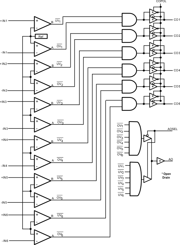
The LMV7231 is Hex Window Comparator which can be used to monitor power supply voltages and other critical system voltage levels.
The LMV7231 contains 6 identical window comparators where the upper and lower trip points are set through external resistor dividers. Each input of the comparator is compared to a internal 1.5% accurate 400-mV reference voltage (VREF).
The 6 window comparator outputs (CO1-CO6) signal an undervoltage or overvoltage event for each power supply input. The COPOL pin sets the inside or outside of the window indication.
A combined OR'ed output (AO) is also provided to signal when any of the power supply inputs have an overvoltage or undervoltage event. AOSEL sets the logic polarity to create a power-good or error signal.
7.2 Functional Block Diagram
7.3 Feature Description
The LMV7231 Hex Window Comparator with 1.5% precision can accurately monitor up to 6 power rails or batteries at one time. The input and output voltages of the device can exceed the supply voltage, V+, of the comparator, and can be up to the maximum ratings listed in the Absolute Maximum Ratings without causing damage or performance degradation. The typical microcontroller input pin with crowbar diode ESD protection circuitry does not allow the input to go above V+, and thus its usefulness is limited in power supply supervision applications.
7.3.1 Input and Output Voltage Range Above V+
The supply independent inputs of the window comparator blocks allow the LMV7231 to be tolerant of system faults. For example, if the power is suddenly removed from the LMV7231 due to a system malfunction while a voltage still exists on the input, it is not an issue as long as the monitored input voltage does not exceed the absolute maximum ratings. Another example where this feature comes in handy is a battery-sense application such as the one in Figure 32. The boards may be sitting on the shelf unbiased with V+ grounded, and yet have a fully charged battery onboard. If the comparator measuring the battery had crowbar diodes, the diode from –IN to V+ would turn on, sourcing current from the battery, eventually draining the battery. However, when using the LMV7231 no current, except the low input bias current of the device, flows into the chip, and the battery charge is preserved.
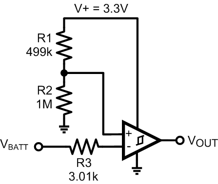 Figure 32. Battery-Sense Application
The output pin voltages of the device can also exceed the supply voltage, V+, of the comparator. This provides extra flexibility and enables designs which pull up the outputs to higher voltage levels to meet system requirements. For example, it is possible to run the LMV7231 at its minimum operating voltage, V+ = 2.2 V, but to bias a blue LED, pull up the output listed in the Absolute Maximum Ratings, with a forward voltage of VF = 4 V.
In a power supply supervision application, the hardwired LMV7231 is a sound solution compared to the microcontroller with software alternative for several reasons. First, start-up is faster. During start-up, code loading time, oscillator ramp time, and reset time do not need to be accounted for. Second, operation is quick. The LMV7231 has a maximum propagation delay and is not affected by sampling and conversion delays related to reading data, calculating data, and setting flags. Third, the device has less overhead. The LMV7231 does not require an expensive power-consuming microcontroller nor is it dependent on controller code which could get damaged or crash.
7.4 Device Functional Modes
7.4.1 +IN1 through +IN6 Input Pins
These inputs set the upper threshold voltage of the channel window comparator. The input voltage is compared to the internal 400-mV reference. These inputs are capable of input voltages up to the Absolute Maximum Ratings (6 V), independent of the V+ supply voltage.
7.4.2 –IN1 through –IN6 Input Pins
These inputs set the lower threshold voltage of the channel window comparator. The input voltage is compared to the internal 400-mV reference. These inputs are capable of input voltages up to the Absolute Maximum Ratings (6 V), independent of the V+ supply voltage.
7.4.3 CO1 through C06 Output Pins
These are the open-drain outputs of the individual comparators. A pullup resistor is required or several outputs may be logic OR'ed together with a common pullup resistor. The polarity is determined by the COPOL input pin setting.
7.4.4 COPOL Input Pin
The state of this comparator output polarity select input pin determines whether the CO1-CO6 pins are active-high or active-low. When tied LOW, the CO1-CO6 outputs go LOW to indicate an out-of-window comparison. When tied HIGH, the outputs go LOW to indicate a within-window comparison.
7.4.5 AO Output Pin
This output is the AND'ed combination of either the overvoltage comparator outputs or the undervoltage comparator outputs and is controlled by the state of the AOSEL. The AO pin is active-low.
7.4.6 AOSEL Input Pin
The state of this AND output level select pin determines whether the AO pin is active on an overvoltage or undervoltage event. When tied LOW the AO output is active upon an overvoltage event.
7.4.7 Three-Resistor Voltage Divider Selection
The LMV7231 trip points can be set by external resistor dividers as shown in Figure 33.
 Figure 33. External Resistor Dividers
Each trip point, overvoltage (VOV) and undervoltage (VUV), can be optimized for a falling supply (VTHF), or a rising supply (VTHR).
Therefore, there are 22 = 4 different optimization cases:
- Exiting the voltage detection window (Figure 34)
- Rising into and out of the window (Figure 35)
- Entering the window (Figure 36)
- Falling into and out of the window (Figure 37)
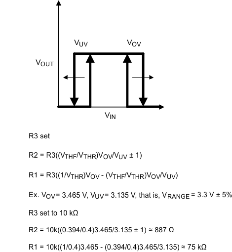 Figure 34. Exiting the Voltage Detection Window
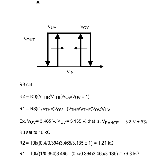 Figure 36. Entering the Voltage Detection Window
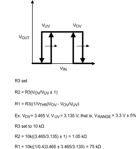 Figure 35. Rising into and out of the Voltage Detection Window
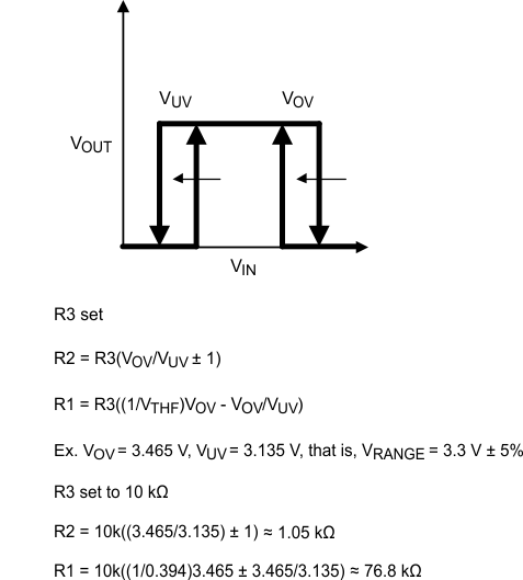 Figure 37. Falling into and out of the Voltage Detection Window
NOTE
For each case, each trip point can be optimized for either a rising or falling signal, but not both.
The governing equations make it such that if the same resistor, R3, and overvoltage-to-undervoltage ratio, VOV/VUV, is used across the channels, the same nominal current travels through the resistor ladder. As a result, R2 is also the same across all channels, and only R1 needs to change to set voltage detection window maximizing reuse of resistor values and minimizing design complexity.
Select the R3 resistor value to be below 100 kΩ so the resistor current through the divider ladder is much greater than the LMV7231 bias current (15 nA worst case, 50 pA typical). If the current traveling through the resistor divider is on the same magnitude of the LMV7231 IBIAS, the IBIAS current creates an error in the circuit and causes trip voltage shifts. The greatest error due to IBIAS is caused when that current passes through the greatest equivalent resistance, REQ = R1‖(R2+R3), which is detected by the positive input of the window comparator, +IN.