SNOSB45F February 2010 – January 2016 LMV7231
PRODUCTION DATA.
- 1 Features
- 2 Applications
- 3 Description
- 4 Revision History
- 5 Pin Configuration and Functions
- 6 Specifications
- 7 Detailed Description
- 8 Application and Implementation
- 9 Power Supply Recommendations
- 10Layout
- 11Device and Documentation Support
- 12Mechanical, Packaging, and Orderable Information
8 Application and Implementation
NOTE
Information in the following applications sections is not part of the TI component specification, and TI does not warrant its accuracy or completeness. TI’s customers are responsible for determining suitability of components for their purposes. Customers should validate and test their design implementation to confirm system functionality.
8.1 Application Information
The LMV7231 is specified for operation from 2.2 V to 5.5 V. Some of the specifications apply from –10°C to +70°C. Parameters that can exhibit significant variance with regard to operating voltage or temperature are presented in the Typical Characteristics and the 3.3-V Electrical Characteristics.
8.2 Typical Application
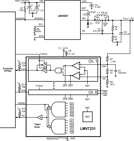
Figure 38 shows a typical power supply supervision circuit using the LMV7231 and the efficient, easy to use LM25007 step-down switching regulator.
8.2.1 Design Requirements
Table 1 describes the requested design parameters.
Table 1. Design Parameters
| PARAMETER | EXAMPLE VALUE | |||
|---|---|---|---|---|
| Logic Supply Voltage | 3.3 V | |||
| Monitored Voltage | 5 V | |||
| Monitored Voltage Tolerance Window | ±5% (4.75 V to 5.25 V) | |||
8.2.2 Detailed Design Procedure
The regulators output voltage is set to 5 V, according to the LM25007 data sheet, SNVS401.
Resistor R6 and capacitors C6, C7 are utilized to minimize output ripple voltage per the AN-1453 LM25007 Evaluation Board, (SNVA152).
The comparator voltage window is set to 5 V ±5%. This requires input voltages of 420 mV and 380 mV, which calculates to R7 = 1.15 kΩ , R8 = 10 Ω, R9 = 95.3 Ω. See the Three-Resistor Voltage Divider Selection section for details on how to set the comparator voltage window.
With the components selected, the output ripple voltage on the LM25007 is approximately 30 to 35 mV and is reduced to about 4 mV at the comparator input, +IN1, by the resistor divider. This ripple voltage can be reduced multiple ways. First, user can operate the device in continuous conduction mode rather than discontinuous conduction mode. To do this increase the load current of the device (see SNVS401 for more details). However, the power rating of the resistors in the resistor ladder must not be exceeded. Second, ripple can be reduced further with a bypass capacitor, C9, at the resistor divider. If desired, select a 1-µF capacitor to achieve less than 3-mV ripple at +IN1. However, there is a trade-off that adding capacitance at this node lowers the system response time.
8.2.3 Application Curve
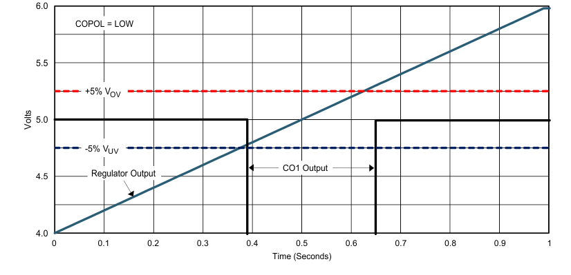
Figure 39 shows the results of sweeping the regulator output voltage through the undervoltage and overvoltage thresholds. COPOL is set LOW so that the output goes LOW while the regulator voltage is within the ±5% thresholds.
 Figure 39. Power Supply Supervisor Thresholds
