ZHCSIN6C August   2018  – October 2019 LMR36015-Q1

PRODUCTION DATA.  

  1. 特性
  2. 应用
  3. 说明
    1.     Device Images
      1.      简化原理图
  4. 修订历史记录
  5. Device Comparison Table
  6. Pin Configuration and Functions
    1.     Pin Functions
  7. Specifications
    1. 7.1 Absolute Maximum Ratings
    2. 7.2 ESD Ratings
    3. 7.3 Recommended Operating Conditions
    4. 7.4 Thermal Information
    5. 7.5 Electrical Characteristics
    6. 7.6 Timing Requirements
    7. 7.7 System Characteristics
    8. 7.8 Typical Characteristics
  8. Detailed Description
    1. 8.1 Overview
    2. 8.2 Functional Block Diagram
    3. 8.3 Feature Description
      1. 8.3.1 Power-Good Flag Output
      2. 8.3.2 Enable and Start-up
      3. 8.3.3 Current Limit and Short Circuit
      4. 8.3.4 Undervoltage Lockout and Thermal Shutdown
    4. 8.4 Device Functional Modes
      1. 8.4.1 Auto Mode
      2. 8.4.2 Forced PWM Operation
      3. 8.4.3 Dropout
      4. 8.4.4 Minimum Switch On-Time
      5. 8.4.5 Spread Spectrum Operation
  9. Application and Implementation
    1. 9.1 Application Information
    2. 9.2 Typical Application
      1. 9.2.1 Design 1: Low Power 24-V, 1.5-A PFM Converter
        1. 9.2.1.1 Design Requirements
        2. 9.2.1.2 Detailed Design Procedure
          1. 9.2.1.2.1  Custom Design With WEBENCH Tools
          2. 9.2.1.2.2  Choosing the Switching Frequency
          3. 9.2.1.2.3  Setting the Output Voltage
            1. 9.2.1.2.3.1 FB for Adjustable Output
          4. 9.2.1.2.4  Inductor Selection
          5. 9.2.1.2.5  Output Capacitor Selection
          6. 9.2.1.2.6  Input Capacitor Selection
          7. 9.2.1.2.7  CBOOT
          8. 9.2.1.2.8  VCC
          9. 9.2.1.2.9  CFF Selection
            1. 9.2.1.2.9.1 External UVLO
          10. 9.2.1.2.10 Maximum Ambient Temperature
      2. 9.2.2 Application Curves
      3. 9.2.3 Design 2: High Density 12-V, 1.5-A FPWM Converter
        1. 9.2.3.1 Design Requirements
        2. 9.2.3.2 Detailed Design Procedure
        3. 9.2.3.3 Application Curves
    3. 9.3 What to Do and What Not to Do
  10. 10Power Supply Recommendations
  11. 11Layout
    1. 11.1 Layout Guidelines
      1. 11.1.1 Ground and Thermal Considerations
    2. 11.2 Layout Example
  12. 12器件和文档支持
    1. 12.1 器件支持
      1. 12.1.1 开发支持
        1. 12.1.1.1 使用 WEBENCH® 工具创建定制设计方案
    2. 12.2 文档支持
      1. 12.2.1 相关文档
    3. 12.3 接收文档更新通知
    4. 12.4 支持资源
    5. 12.5 商标
    6. 12.6 静电放电警告
    7. 12.7 Glossary
  13. 13机械、封装和可订购信息

封装选项

机械数据 (封装 | 引脚)
散热焊盘机械数据 (封装 | 引脚)
订购信息

Application Curves

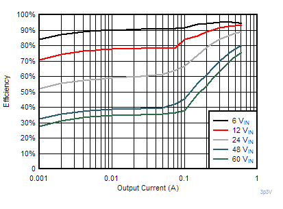
Unless otherwise specified the following conditions apply: VIN = 24 V, TA = 25°C. The circuit is shown in Figure 18, with the appropriate BOM from Table 5.
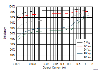
LMR36015-Q1 3p3Vout-efficiency-400khz-600ma.gif
VOUT = 5 V 400 kHz
Figure 22. Efficiency
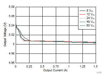
LMR36015-Q1 LMR36015A_5Vout_LoadReg-rtm.gif
VOUT = 5 V 400 kHz
Figure 24. Load Regulation
LMR36015-Q1 LMR36015A_5Vout_LineReg.gif
VOUT = 5 V 400 kHz
Figure 26. Line Regulation
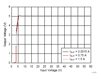
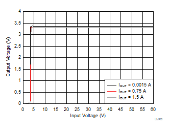
LMR36015-Q1 LMR36015A_5Vout_Dropout-rtm.gif
VOUT = 5 V 400 kHz
Figure 28. Overall Dropout Characteristic
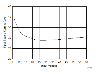
LMR36015-Q1 LMR36015A_Input_Current.gif
VOUT = 3.3 V IOUT= 0 A RFBT= 100 kΩ
Figure 30. Input Supply Current
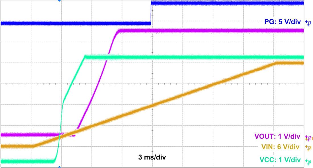
LMR36015-Q1 waveform-01-LMR36015A-24VIN-5VOUT-STARTUP-SNVSAY8.jpg
VOUT = 5 V 400 kHz
Figure 32. Start-Up Waveform
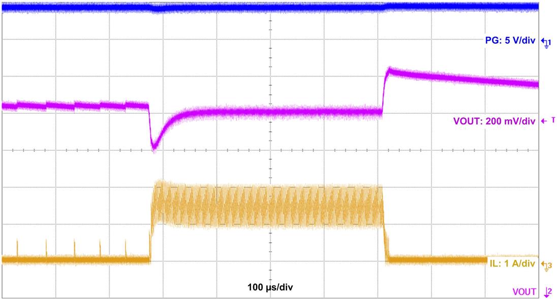
LMR36015-Q1 waveform-08-LMR36015A-24VIN-5VOUT-LT-1P5MA-SNVSAY8.jpg
VOUT = 5 V 400 kHz ILOAD= 10 mA - 0.75 A
Slew Rate = 1 µs/A
Figure 34. Load Transient
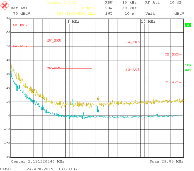
LMR36015-Q1 conducted_low.gif
VIN = 13.5 V VOUT = 5 V IOUT = 1.5 A
Frequency Tested: 150 kHz to 30 MHz
Figure 36. Conducted EMI vs. CISPR25 Limits (Yellow: Peak Signal, Blue: Average Signal)
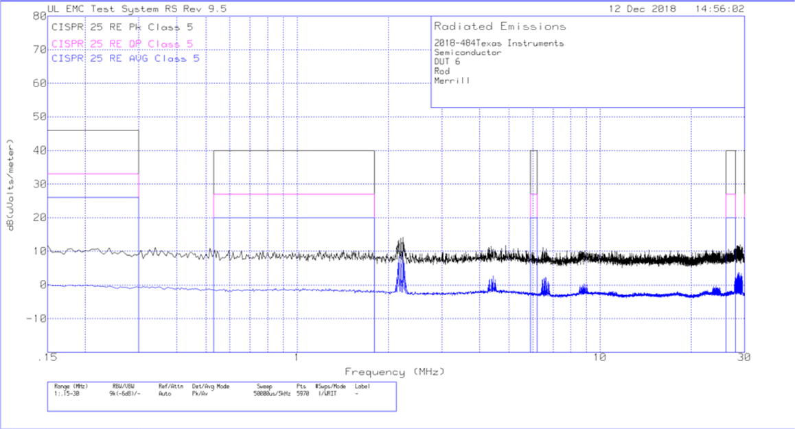
LMR36015-Q1 rod.gif
VIN = 13.5 V VOUT = 5 V IOUT = 1.5 A
Frequency Tested: 150 kHz to 30 MHz
Figure 38. Radiated EMI Rod vs. CISPR25 Limits
LMR36015-Q1 bicon_horizontal.gif
VIN = 13.5 V VOUT = 5 V IOUT = 1.5 A
Frequency Tested: 30 MHz to 200 MHz
Figure 40. Radiated EMI Bicon Horizontal vs. CISPR25 Limits
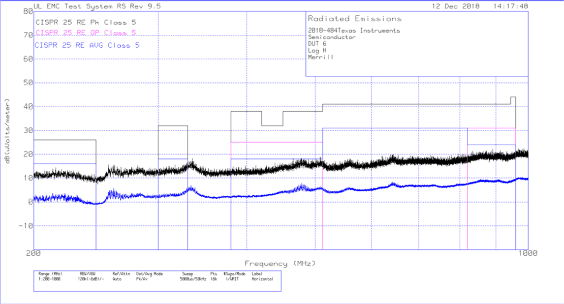
LMR36015-Q1 log_horizaontal.gif
VIN = 13.5 V VOUT = 5 V IOUT = 1.5 A
Frequency Tested: 200 MHz to 1 GHz
Figure 42. Radiated EMI Log Horizontal vs. CISPR25 Limits
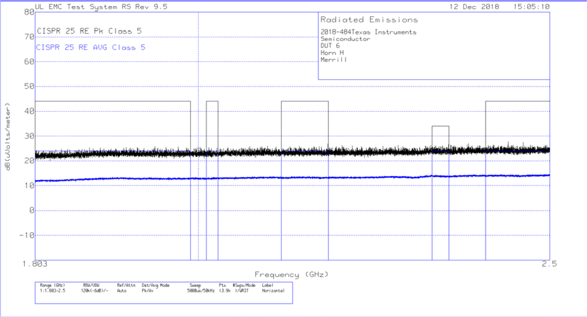
LMR36015-Q1 horn_horizontal.gif
VIN = 13.5 V VOUT = 5 V IOUT = 1.5 A
Frequency Tested: 1.8 GHz to 2.5 GHz
Figure 44. Radiated EMI Horn Horizontal vs. CISPR25 Limits
LMR36015-Q1 LMR36015A_3p3Vout_Efficiency-rtm.gif
VOUT = 3.3 V 400 kHz
Figure 23. Efficiency
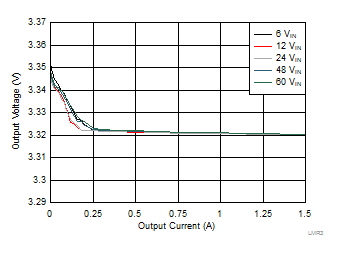
LMR36015-Q1 LMR36015A_3p3Vout_LoadReg-rtm.gif
VOUT = 3.3 V 400 kHz
Figure 25. Load Regulation
LMR36015-Q1 LMR36015A_3P3Vout_LineReg.gif
VOUT = 3.3 V 400 kHz
Figure 27. Line Regulation
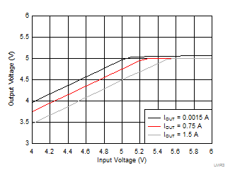
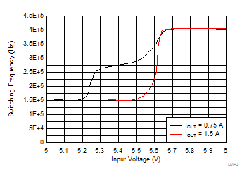
LMR36015-Q1 LMR36015A_Frequency_DropOut.gif
VOUT = 5 V 400 kHz
Figure 29. Frequency Dropout Characteristic
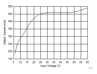
LMR36015-Q1 LMR36015A-PFM-CCM.gif
VOUT = 3.3 V 400 kHz
Figure 31. Mode Change Thresholds
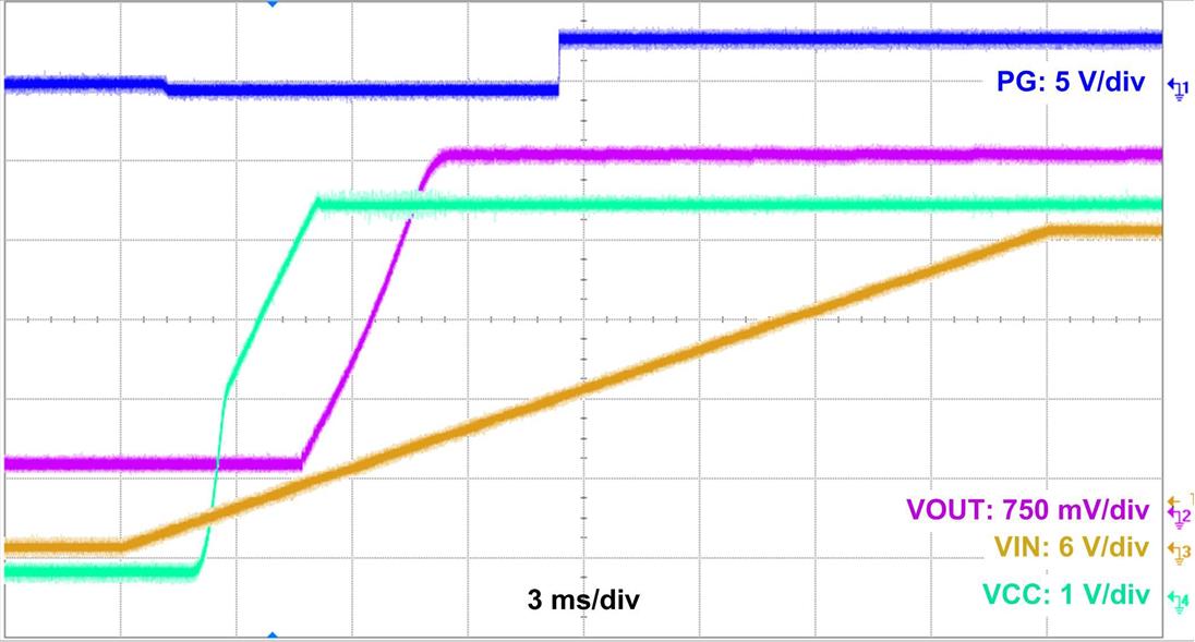
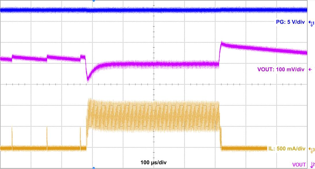
LMR36015-Q1 waveform-04-LMR36015A-24VIN-3P3VOUT-STARTUP-SNVSAY8.jpg
VOUT = 3.3 V 400 kHz
Figure 33. Start-Up Waveform
LMR36015-Q1 waveform-10-LMR36015A-24VIN-3P3VOUT-LT-750MA-SNVSAY8.jpg
VOUT = 3.3 V 400 kHz ILOAD= 10 mA - 0.75 A
Slew Rate = 1 µs/A
Figure 35. Load Transient
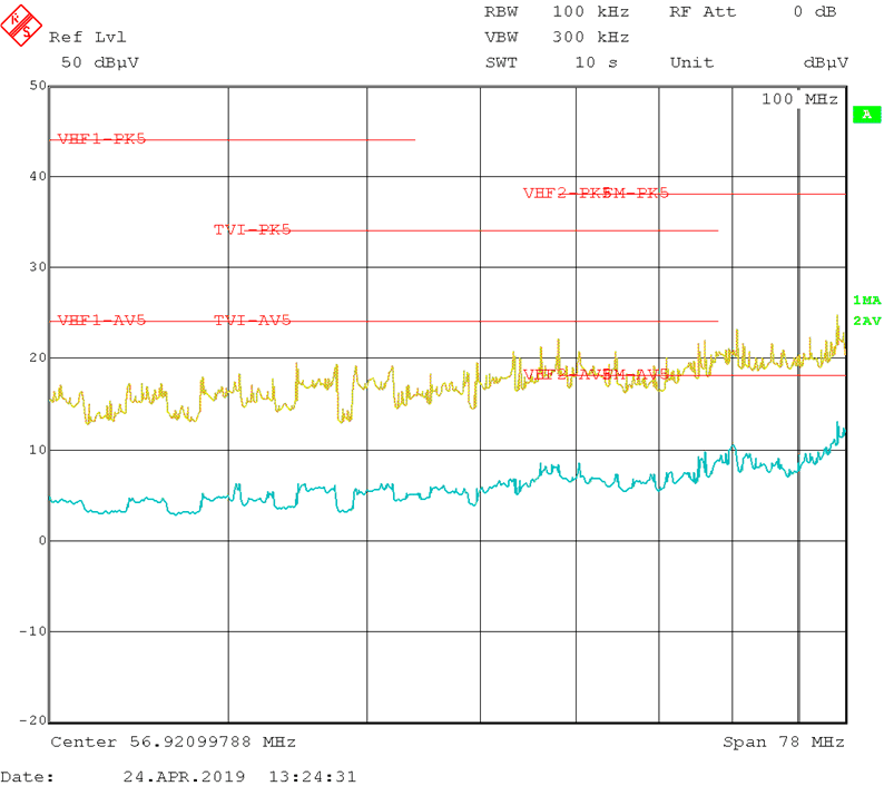
LMR36015-Q1 conducted_high.gif
VIN = 13.5 V VOUT = 5 V IOUT = 1.5 A
Frequency Tested: 30 MHz to 108 MHz
Figure 37. Conducted EMI vs. CISPR25 Limits (Yellow: Peak Signal, Blue: Average Signal)
LMR36015-Q1 bicon_vert.gif
VIN = 13.5 V VOUT = 5 V IOUT = 1.5 A
Frequency Tested: 30 MHz to 200 MHz
Figure 39. Radiated EMI Bicon Vertical vs. CISPR25 Limits
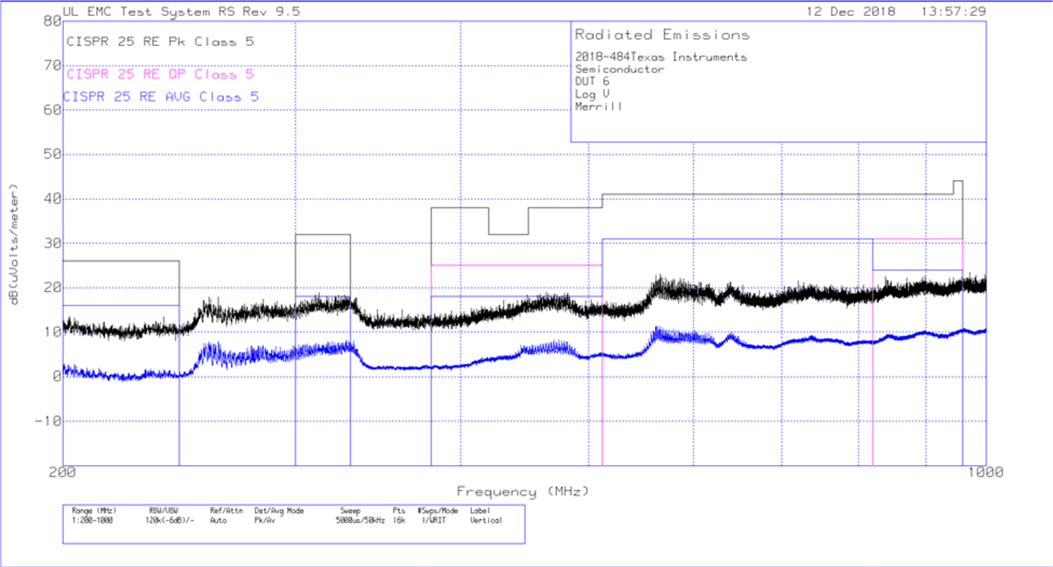
LMR36015-Q1 log_vertical.gif
VIN = 13.5 V VOUT = 5 V IOUT = 1.5 A
Frequency Tested: 200 MHz to 1 GHz
Figure 41. Radiated EMI Log Vertical vs. CISPR25 Limits
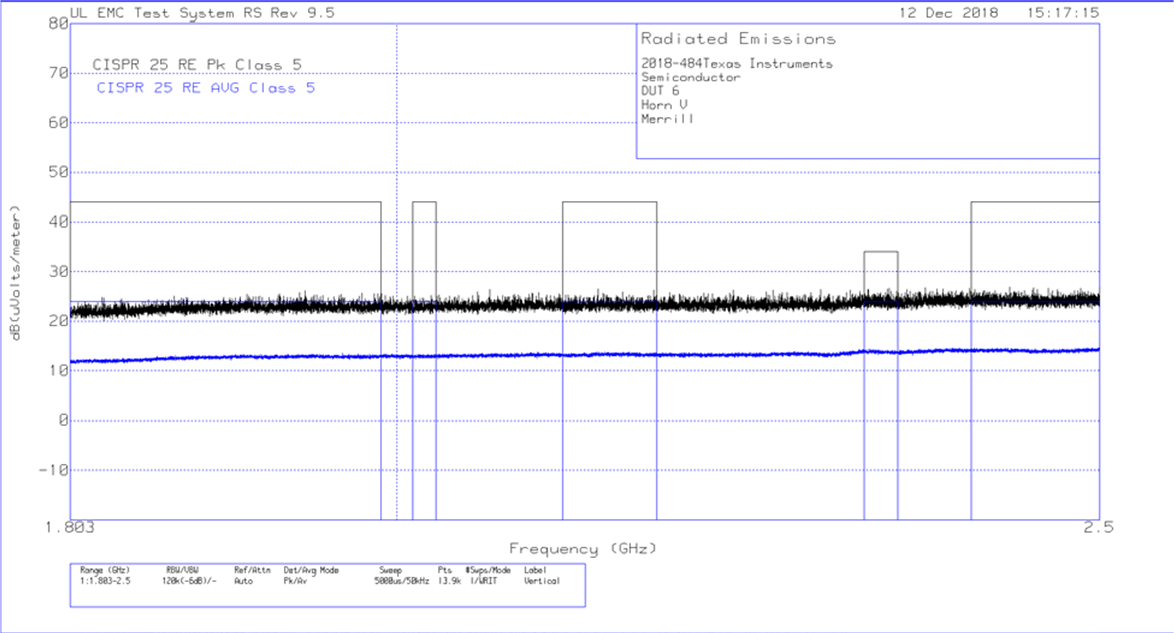
LMR36015-Q1 horn_vertical.gif
VIN = 13.5 V VOUT = 5 V IOUT = 1.5 A
Frequency Tested: 1.83 GHz to 2.5 GHz
Figure 43. Radiated EMI Horn Vertical vs. CISPR25 Limits
LMR36015-Q1 lmr342xx-emi-schematic-snvsba9.gif
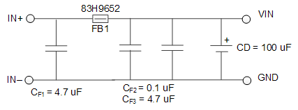
Figure 45. Recommended Input EMI Filter