SNVSA10B November 2013 – November 2014 LMR14006
PRODUCTION DATA.
- 1 Features
- 2 Applications
- 3 Description
- 4 Revision History
- 5 Pin Configuration and Functions
- 6 Specifications
- 7 Detailed Description
- 8 Applications and Implementation
- 9 Layout
- 10Mechanical, Packaging, and Orderable Information
5 Pin Configuration and Functions
DDC Package
TSOP-6L
Top View
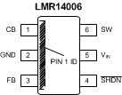
Pin Functions
| PIN | I/O | DESCRIPTION | |
|---|---|---|---|
| NAME | NUMBER | ||
| CB | 1 | I | SW FET Gate Bias voltage. Connect Cboot cap between CB and SW |
| GND | 2 | G | Ground Connection |
| FB | 3 | I | Feedback Pin. Set feedback voltage divider ratio with VOUT = VFB (1+(R1/R2)) |
| /SHDN | 4 | I | Enable and disable input pin(high voltage tolerant). Internal pull-up current source. Pull below 1.2V to disable. Float to enable. Adjust the input undervoltage lockout with two resistors. |
| VIN | 5 | I | Power input voltage pin. Input for internal supply and drain node input for internal high-side MOSFET |
| SW | 6 | O | Switch node. Connect to inductor, diode, and Cboot cap |