ZHCSA20C October   2011  – June 2019 LMR10510

PRODUCTION DATA.  

  1. 特性
  2. 应用
  3. 说明
    1.     Device Images
      1.      简化应用
  4. 修订历史记录
  5. 说明(续)
  6. Pin Configuration and Functions
    1.     Pin Description: 5-Pin SOT-23
    2.     Pin Descriptions 6-Pin WSON
  7. Specifications
    1. 7.1 Absolute Maximum Ratings
    2. 7.2 Recommended Operating Ratings
    3. 7.3 Electrical Characteristics
    4. 7.4 Typical Performance Characteristics
  8. Detailed Description
    1. 8.1 Overview
    2. 8.2 Functional Block Diagram
    3. 8.3 Feature Description
      1. 8.3.1 Soft Start
      2. 8.3.2 Output Overvoltage Protection
      3. 8.3.3 Undervoltage Lockout
      4. 8.3.4 Current Limit
      5. 8.3.5 Thermal Shutdown
  9. Application and Implementation
    1. 9.1 Application Information
    2. 9.2 Typical Application
      1. 9.2.1 Detailed Design Procedure
        1. 9.2.1.1 Custom Design With WEBENCH® Tools
        2. 9.2.1.2 Inductor Selection
        3. 9.2.1.3 Input Capacitor
        4. 9.2.1.4 Output Capacitor
        5. 9.2.1.5 Catch Diode
        6. 9.2.1.6 Output Voltage
        7. 9.2.1.7 Calculating Efficiency, and Junction Temperature
      2. 9.2.2 Application Curves
      3. 9.2.3 Other System Examples
        1. 9.2.3.1 LMR10510x Design Example 1
        2. 9.2.3.2 Lmr10510X Design Example 2
        3. 9.2.3.3 LMR10510Y Design Example 3
        4. 9.2.3.4 LMR10510Y Design Example 4
  10. 10Layout
    1. 10.1 Layout Guidelines
    2. 10.2 Layout Example
    3. 10.3 Thermal Definitions
    4. 10.4 WSON Package
  11. 11器件和文档支持
    1. 11.1 器件支持
      1. 11.1.1 开发支持
        1. 11.1.1.1 使用 WEBENCH® 工具创建定制设计
    2. 11.2 接收文档更新通知
    3. 11.3 社区资源
    4. 11.4 商标
    5. 11.5 静电放电警告
    6. 11.6 Glossary
  12. 12机械、封装和可订购信息

封装选项

机械数据 (封装 | 引脚)
散热焊盘机械数据 (封装 | 引脚)
订购信息

Typical Performance Characteristics

Unless stated otherwise, all curves taken at VIN = 5 V with configuration in typical application circuit shown in Figure 15. TJ = 25°C, unless otherwise specified.
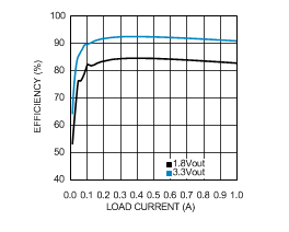
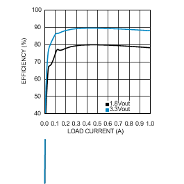
LMR10510 30165696.gif
VIN = 5 V VOUT = 1.8 V and 3.3 V
Figure 1. Η vs Load "X"
LMR10510 30165698.gif
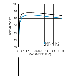
VIN = 3.3 V VOUT = 1.8 V
Figure 3. Η vs Load "X And Y"
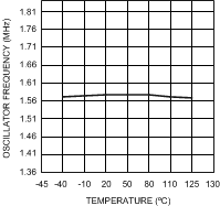
LMR10510 30165636.gif
Figure 5. Oscillator Frequency vs Temperature - "Y"
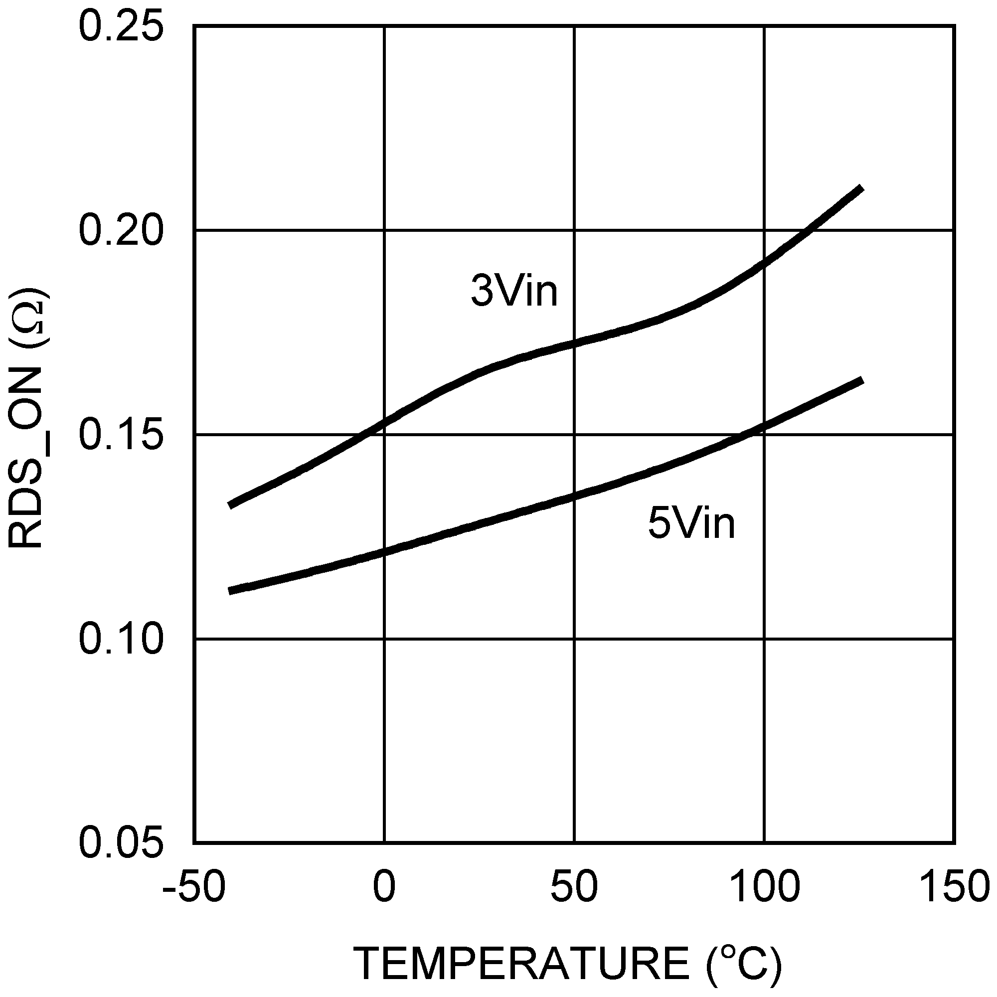
LMR10510 30165687.png
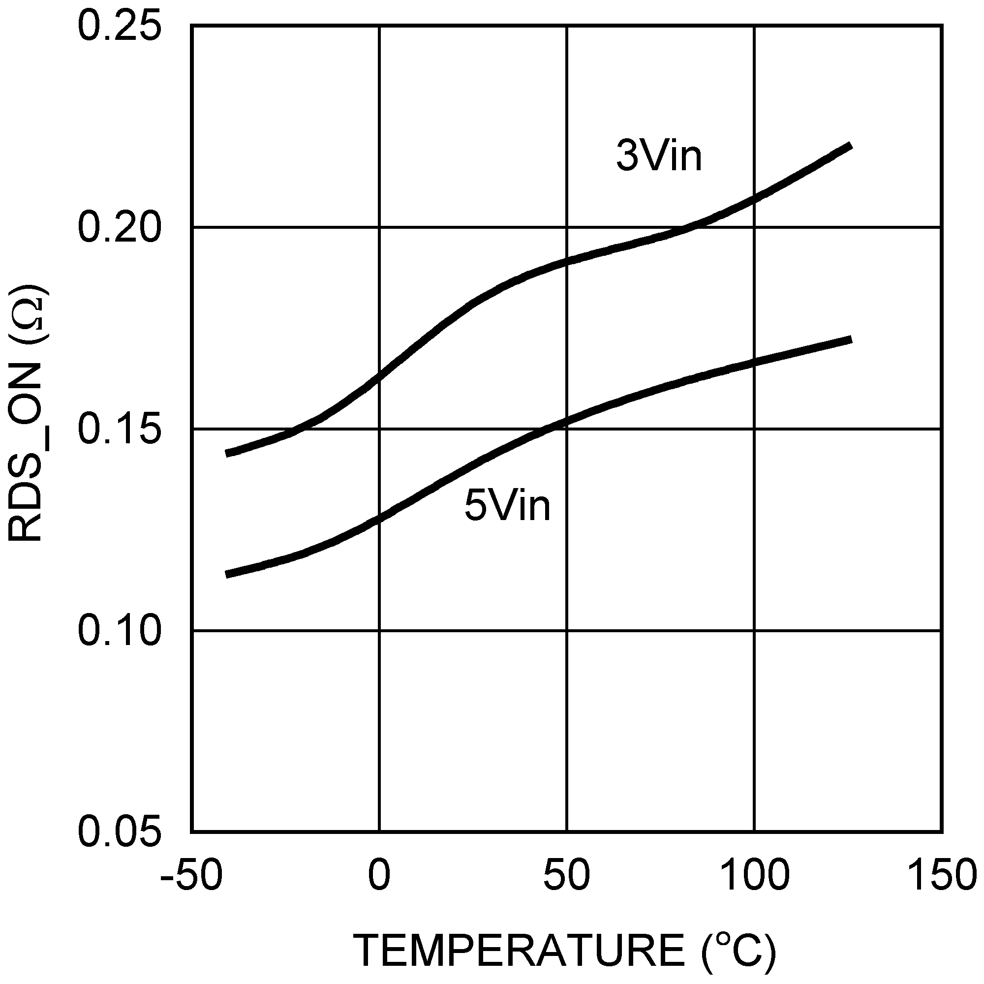
Figure 7. RDSON vs Temperature (WSON Package)
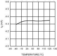
LMR10510 30165628.gif
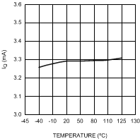
Figure 9. LMR10510X IQ (Quiescent Current)
LMR10510 30165627.gif
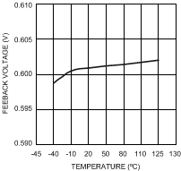
Figure 11. VFB vs Temperature
LMR10510 30165657.png
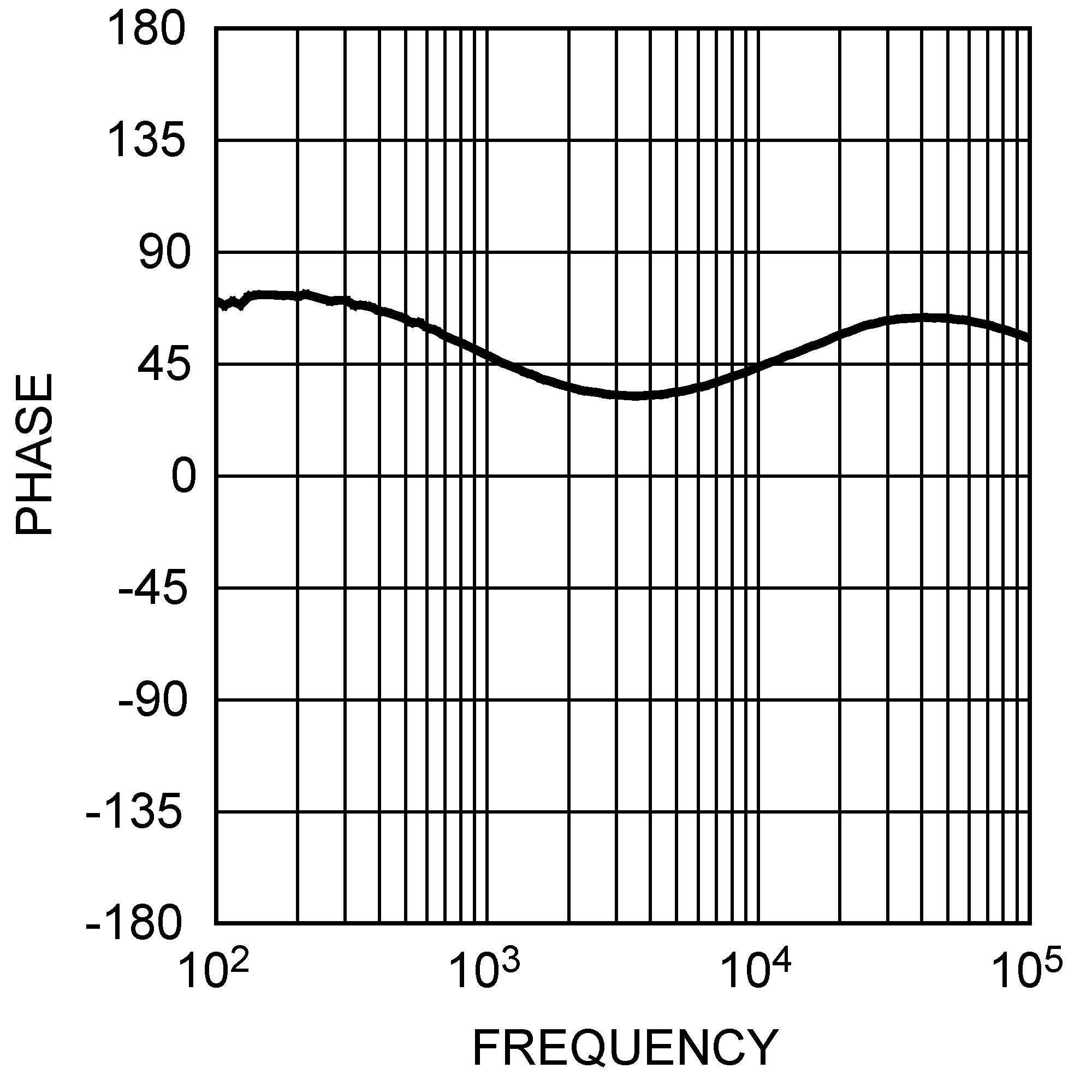
VIN = 5 V VOUT = 1.2 V at 1 A
Figure 13. Phase Plot vs Frequency
LMR10510 30165697.gif
VIN = 5 V VOUT = 1.8 V and 3.3 V
Figure 2. Η vs Load "Y"
LMR10510 30165624.gif
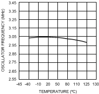
Figure 4. Oscillator Frequency vs Temperature - "X"
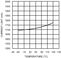
LMR10510 30165686.gif
VIN = 3.3 V
Figure 6. Current Limit vs Temperature
LMR10510 30165688.png
Figure 8. RDSON vs Temperature (Sot-23 Package)
LMR10510 30165637.gif
Figure 10. LMR10510Y IQ (Quiescent Current)
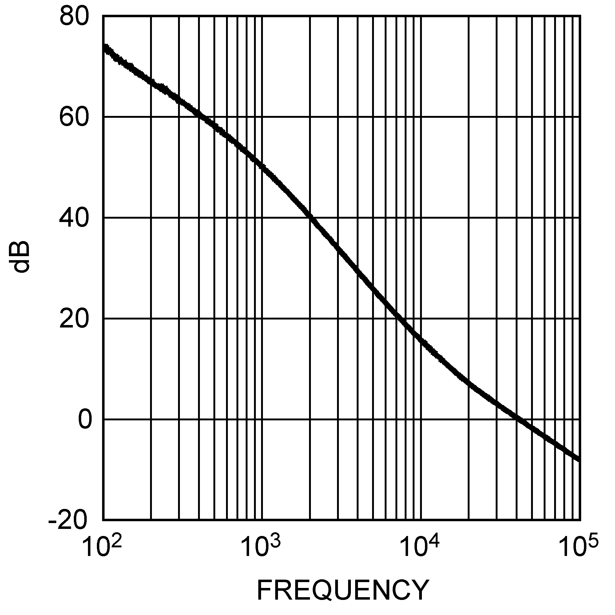
LMR10510 30165656.png
VIN = 5 V VOUT = 1.2 V at 1 A
Figure 12. Gain vs Frequency