SNOSB28G August 2010 – November 2014 LMP8640 , LMP8640-Q1 , LMP8640HV
PRODUCTION DATA.
- 1 Features
- 2 Applications
- 3 Description
- 4 Revision History
- 5 Device Comparison Table
- 6 Pin Configuration and Functions
-
7 Specifications
- 7.1 Absolute Maximum Ratings
- 7.2 Handling Ratings - LMP8640, LMP8640HV
- 7.3 Handling Ratings - LMP8640-Q1
- 7.4 Recommended Operating Conditions
- 7.5 Thermal Information
- 7.6 Electrical Characteristics 2.7 V
- 7.7 Electrical Characteristics 5 V
- 7.8 Electrical Characteristics 12 V
- 7.9 Typical Characteristics
- 8 Detailed Description
- 9 Application and Implementation
- 10Power Supply Recommendations
- 11Layout
- 12Device and Documentation Support
- 13Mechanical, Packaging, and Orderable Information
6 Pin Configuration and Functions
6-Pin SOT-23
DDC0006A Package
(Top View)
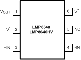
Pin Functions
| PIN | DESCRIPTION | |
|---|---|---|
| NUMBER | NAME | |
| 1 | VOUT | Output |
| 2 | V- | Negative Supply Voltage |
| 3 | +IN | Positive Input |
| 4 | -IN | Negative Input |
| 5 | NC | Not Internally Connected |
| 6 | V+ | Positive Supply Voltage |