SNOSB28G August 2010 – November 2014 LMP8640 , LMP8640-Q1 , LMP8640HV
PRODUCTION DATA.
- 1 Features
- 2 Applications
- 3 Description
- 4 Revision History
- 5 Device Comparison Table
- 6 Pin Configuration and Functions
-
7 Specifications
- 7.1 Absolute Maximum Ratings
- 7.2 Handling Ratings - LMP8640, LMP8640HV
- 7.3 Handling Ratings - LMP8640-Q1
- 7.4 Recommended Operating Conditions
- 7.5 Thermal Information
- 7.6 Electrical Characteristics 2.7 V
- 7.7 Electrical Characteristics 5 V
- 7.8 Electrical Characteristics 12 V
- 7.9 Typical Characteristics
- 8 Detailed Description
- 9 Application and Implementation
- 10Power Supply Recommendations
- 11Layout
- 12Device and Documentation Support
- 13Mechanical, Packaging, and Orderable Information
7 Specifications
7.1 Absolute Maximum Ratings(1)(2)(3)
LMP8640 limits also apply to the LMP8640-Q1.| MIN | MAX | UNIT | |||
|---|---|---|---|---|---|
| Supply Voltage (VS = V+ - V−) | -0.3 | 13.2 | V | ||
| Differential Voltage +IN- (-IN) | -6 | 6 | V | ||
| Voltage at pins +IN, -IN | LMP8640HV | -6 | 80 | V | |
| LMP8640, LMP8640-Q1 | -6 | 60 | V | ||
| Voltage at VOUT pin | V- | V+ | V | ||
| Junction Temperature (4) | -40 | 150 | °C | ||
(1) “Absolute Maximum Ratings” indicate limits beyond which damage to the device may occur, including inoperability and degradation of device reliability and/or performance. Functional operation of the device and/or non-degradation at the Absolute Maximum Ratings or other conditions beyond those indicated in the Operating Ratings is not implied. Operating Ratings indicate conditions at which the device is functional and the device should not be operated beyond such conditions.
(2) For soldering specifications,see product folder at www.ti.com and http://www.ti.com/lit/SNOA549.
(3) If Military/Aerospace specified devices are required, please contact the Texas Instruments Sales Office/Distributors for availability and specifications.
(4) The maximum power dissipation must be derated at elevated temperatures and is dictated by TJ(MAX), θJA, and the ambient temperature, TA. The maximum allowable power dissipation PDMAX = (TJ(MAX) - TA)/ θJA or the number given in Absolute Maximum Ratings, whichever is lower.
7.2 Handling Ratings - LMP8640, LMP8640HV
| MIN | MAX | UNIT | ||||
|---|---|---|---|---|---|---|
| Tstg | Storage temperature range | -65 | 150 | °C | ||
| V(ESD) | Electrostatic discharge | Human body model (HBM(1)) | For input pins +IN, -IN | -5000 | 5000 | V |
| For all other pins | -2000 | 2000 | ||||
| Charged device model (CDM)(2) | All pins | -1250 | 1250 | |||
| Machine model (MM) (3) | -200 | 200 | ||||
(1) JEDEC document JEP155 states that 500-V HBM allows safe manufacturing with a standard ESD control process.
(2) JEDEC document JEP157 states that 250-V CDM allows safe manufacturing with a standard ESD control process.
(3) Machine Model, applicable std. JESD22-A115-A (ESD MM std. of JEDEC)
7.3 Handling Ratings - LMP8640-Q1
| MIN | MAX | UNIT | ||||
|---|---|---|---|---|---|---|
| Tstg | Storage temperature range | -65 | 150 | °C | ||
| V(ESD) | Electrostatic discharge | Human body model (HBM), per AEC Q100-002(1) | -2000 | 2000 | V | |
| Charged device model (CDM), per AEC Q100-011 | All pins | -1000 | 1000 | |||
| Machine model (MM) (2) | All pins | -200 | 200 | |||
(1) AEC Q100-002 indicates HBM stressing is done in accordance with the ANSI/ESDA/JEDEC JS-001 specification.
(2) Machine Model, applicable std. JESD22-A115-A (ESD MM std. of JEDEC)
7.4 Recommended Operating Conditions(1)
| MIN | MAX | UNIT | |
|---|---|---|---|
| Supply Voltage (VS = V+ - V−) | 2.7 | 12 | V |
| Operating Junction Temperature Range (4) | -40 | 125 | °C |
7.5 Thermal Information
| THERMAL METRIC(1) | LMP8640 LMP8640HV LMP8640-Q1 |
UNIT | |
|---|---|---|---|
| THIN SOT-23 | |||
| 6 PINS | |||
| RθJA | Junction-to-ambient thermal resistance (4) | 165 | °C/W |
| RθJC(top) | Junction-to-case (top) thermal resistance | 28 | |
| RθJB | Junction-to-board thermal resistance | 24.6 | |
| ψJT | Junction-to-top characterization parameter | 0.3 | |
| ψJB | Junction-to-board characterization parameter | 23.8 | |
(1) For more information about traditional and new thermal metrics, see the IC Package Thermal Metrics application report, SPRA953.
7.6 Electrical Characteristics 2.7 V (1)
Unless otherwise specified, all limits ensured for at TA = 25°C, VS= V+ – V-, VSENSE= +IN-(-IN), V+ = 2.7 V, V− = 0 V, −2 V < VCM < 76 V, RL = 10 MΩ. LMP8640 limits also apply to the LMP8640-Q1.| PARAMETER | TEST CONDITIONS | MIN(3) | TYP(2) | MAX(3) | UNIT | |
|---|---|---|---|---|---|---|
| VOS | Input Offset Voltage | VCM = 2.1 V | -900 | 900 | µV | |
| VCM = 2.1 V, Over Temperature | -1160 | 1160 | ||||
| TCVOS | Input Offset Voltage Drift(4)(6) | VCM = 2.1 V | 2.6 | µV/°C | ||
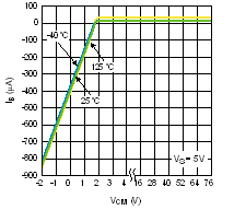
| IB | Input Bias Current (7) | VCM = 2.1 V, VSENSE = 0 V | 12 | 20 | µA | |
| VCM = 2.1 V, Over Temperature, VSENSE = 0 V | 27 | |||||
| eni | Input Voltage Noise (6) | f > 10 kHz | 117 | nV/√Hz | ||
| Gain AV | Gain LMP8640-T LMP8640HV-T | 20 | V/V | |||
| Gain LMP8640-F LMP8640HV-F | 50 | |||||
| Gain LMP8640-H LMP8640HV-H | 100 | |||||
| Gain error | VCM = 2.1 V | -0.25% | 0.25% | |||
| VCM = 2.1 V, Over Temperature | -0.51% | 0.51% | ||||
| Accuracy over temperature(6) | VCM = 2.1V, Over Temperature | 26.2 | ppm/°C | |||
| PSRR | Power Supply Rejection Ratio | VCM = 2.1 V, 2.7 V < V+ < 12 V, | 85 | dB | ||
| CMRR | Common Mode Rejection Ratio | LMP8640HV 2.1 V < VCM < 42 V LMP8640 2.1 V < VCM< 42 V |
103 | dB | ||
| LMP8640HV 2.1 V < VCM < 76 V | 95 | |||||
| -2 V <VCM < 2 V, | 60 | |||||
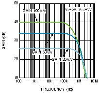
| BW | Fixed Gain LMP8640-T LMP8640HV-T (6) | DC VSENSE = 67.5 mV, CL = 30 pF,RL= 1MΩ |
950 | kHz | ||
| Fixed Gain LMP8640-F LMP8640HV-F (6) | DC VSENSE =27 mV, CL = 30 pF, RL= 1MΩ |
450 | ||||
| Fixed Gain LMP8640-H LMP8640HV-H (6) | DC VSENSE = 13.5 mV, CL = 30 pF ,RL= 1 MΩ |
230 | ||||
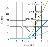
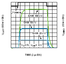
| SR | Slew Rate (5)(6) | VCM =5 V, CL = 30 pF, RL = 1 MΩ, LMP8640-T LMP8640HV-T VSENSE =100 mVpp, LMP8640-F LMP8640HV-F VSENSE =40 mVpp, LMP8640-H LMP8640HV-H VSENSE =20 mVpp, |
1.4 | V/µs | ||
| RIN | Differential Mode Input Impedance(6) | 5 | kΩ | |||
| IS | Supply Current | VCM = 2.1 V | 420 | 600 | µA | |
| VCM = 2.1 V, Over Temperature | 800 | |||||
| VCM = −2 V | 2000 | 2500 | ||||
| VCM = −2 V, Over Temperature | 2750 | |||||
| VOUT | Maximum Output Voltage | VCM = 2.1 V | 2.65 | V | ||
| Minimum Output Voltage | LMP8640-T LMP8640HV-T VCM = 2.1 V |
18.2 | mV | |||
| LMP8640-F LMP8640HV-F VCM = 2.1 V |
40 | |||||
| LMP8640-H LMP8640HV-H VCM = 2.1 V |
80 | |||||
| CLOAD | Max Output Capacitance Load(6) | 30 | pF | |||
(1) Electrical Table values apply only for factory testing conditions at the temperature indicated. Factory testing conditions result in very limited self-heating of the device such that TJ = TA. No specification of parametric performance is indicated in the electrical tables under conditions of internal self-heating where TJ > TA. Absolute Maximum Ratings indicate junction temperature limits beyond which the device may be permanently degraded, either mechanically or electrically.
(2) Typical values represent the most likely parametric norm at the time of characterization. Actual typical values may vary over time and will also depend on the application and configuration. The typical values are not tested and are not ensured on shipped production material.
(3) Limits are 100% production tested at 25°C. Limits over the operating temperature range are ensured through correlations using statistical quality control (SQC) method.
(4) Offset voltage temperature drift is determined by dividing the change in VOS at the temperature extremes by the total temperature change.
(5) The number specified is the average of rising and falling slew rates and measured at 90% to 10%.
(6) This parameter is ensured by design and/or characterization and is not tested in production.
(7) Positive Bias Current corresponds to current flowing into the device. Spec does not include input signal dependent currents on the positive input of approximately Vsense / 5KΩ due to topology feedback action.
7.7 Electrical Characteristics 5 V (1)
Unless otherwise specified, all limits ensured for at TA = 25°C, VS= V+ – V-, VSENSE= +IN-(-IN), V+ = 5 V, V− = 0 V, −2 V < VCM < 76 V, RL = 10 MΩ. LMP8640 electrical limits also apply to the LMP8640-Q1 unless noted.| PARAMETER | TEST CONDITIONS | MIN(3) | TYP(2) | MAX(3) | UNIT | |
|---|---|---|---|---|---|---|
| VOS | Input Offset Voltage | VCM = 2.1 V | -900 | 900 | µV | |
| VCM = 2.1 V, Over Temperature | -1160 | 1160 | ||||
| TCVOS | Input Offset Voltage Drift(4)(6) | VCM = 2.1 V | 2.6 | µV/°C | ||
| IB | Input Bias Current (7) | VCM = 2.1 V, VSENSE = 0 V | 13 | 21 | µA | |
| VCM = 2.1 V, Over Temperature,VSENSE = 0 V | 28 | |||||
| eni | Input Voltage Noise (6) | f > 10 kHz | 117 | nV/√Hz | ||
| Gain AV | Gain LMP8640-T LMP8640HV-T | 20 | V/V | |||
| Gain LMP8640-F LMP8640HV-F | 50 | |||||
| Gain LMP8640-H LMP8640HV-H | 100 | |||||
| Gain error | VCM = 2.1 V | -0.25% | 0.25% | |||
| VCM = 2.1 V, Over Temperature | -0.51% | 0.51% | ||||
| Accuracy over temperature(6) | −40°C to 125°C, VCM=2.1 V | 26.2 | ppm/°C | |||
| PSRR | Power Supply Rejection Ratio | VCM = 2.1 V, 2.7V < V+ < 12 V, | 85 | dB | ||
| CMRR | Common Mode Rejection Ratio | LMP8640HV 2.1 V < VCM < 42 V LMP8640 2.1 V < VCM< 42 V |
103 | dB | ||
| LMP8640HV 2.1 V < VCM < 76 V | 95 | |||||
| -2 V <VCM < 2 V, | 60 | |||||
| BW | Fixed Gain LMP8640-T LMP8640HV-T (6) | DC VSENSE = 67.5 mV, CL = 30 pF ,RL= 1 MΩ |
950 | kHz | ||
| Fixed Gain LMP8640-F LMP8640HV-F(6) | DC VSENSE =27 mV, CL = 30 pF ,RL= 1 MΩ |
450 | ||||
| Fixed Gain LMP8640-H LMP8640HV-H(6) | DC VSENSE = 13.5 mV, CL = 30 pF ,RL= 1MΩ |
230 | ||||
| SR | Slew Rate (5)(6) | VCM =5 V, CL = 30 pF, RL = 1MΩ, LMP8640-T LMP8640HV-T VSENSE = 200 mVpp, LMP8640-F LMP8640HV-F VSENSE = 80 mVpp, LMP8640-H LMP8640HV-H VSENSE = 40 mVpp, |
1.6 | V/µs | ||
| RIN | Differential Mode Input Impedance(6) | 5 | kΩ | |||
| IS | Supply Current | VCM = 2.1 V | 500 | 722 | µA | |
| VCM = 2.1 V, Over Temperature | 922 | |||||
| VCM = −2 V | 2050 | 2500 | ||||
| VCM = −2 V, Over Temperature | 2750 | |||||
| VOUT | Maximum Output Voltage | VCM = 2.1 V | 4.95 | V | ||
| Minimum Output Voltage | LMP8640-T LMP8640HV-T VCM = 2.1 V |
18.2 | mV | |||
| LMP8640-F LMP8640HV-F VCM = 2.1 V |
40 | |||||
| LMP8640-H LMP8640HV-H VCM = 2.1 V |
80 | |||||
| CLOAD | Max Output Capacitance Load(6) | 30 | pF | |||
7.8 Electrical Characteristics 12 V (1)
Unless otherwise specified, all limits ensured for at TA = 25°C, VS= V+ – V-, VSENSE= +IN-(-IN), V+ = 12 V, V− = 0V, −2 V < VCM < 76 V, RL = 10 MΩ. LMP8640 electrical limits also apply to the LMP8640-Q1 unless noted.| PARAMETER | TEST CONDITIONS | MIN(3) | TYP(2) | MAX(3) | UNIT | |
|---|---|---|---|---|---|---|
| VOS | Input Offset Voltage | VCM = 2.1 V | -900 | 900 | µV | |
| VCM = 2.1 V, Over Temperature | -1160 | 1160 | ||||
| TCVOS | Input Offset Voltage Drift(4)(6) | VCM = 2.1 V | 2.6 | µV/°C | ||
| IB | Input Bias Current (7) | VCM = 2.1 V, VSENSE = 0 V | 13 | 22 | µA | |
| VCM = 2.1 V, Over Temperature, VSENSE = 0 V | 28 | |||||
| eni | Input Voltage Noise (6) | f > 10 kHz | 117 | nV/√Hz | ||
| Gain AV | Gain LMP8640-T LMP8640HV-T | 20 | V/V | |||
| Gain LMP8640-F LMP8640HV-F | 50 | |||||
| Gain LMP8640-H LMP8640HV-H | 100 | |||||
| Gain error | VCM = 2.1 V | -0.25% | 0.25% | |||
| VCM = 2.1 V, Over Temperature | -0.51% | 0.51% | ||||
| Accuracy over temperature(6) | −40°C to 125°C, VCM= 2.1 V | 26.2 | ppm/°C | |||
| PSRR | Power Supply Rejection Ratio | VCM = 2.1 V, 2.7 V < V+ < 12 V, | 85 | dB | ||
| CMRR | Common Mode Rejection Ratio | LMP8640HV 2.1 V < VCM < 42 V LMP8640 2.1 V < VCM< 42 V |
103 | dB | ||
| LMP8640HV 2.1 V < VCM < 76 V | 95 | |||||
| -2 V < VCM < 2 V, | 60 | |||||
| BW | Fixed Gain LMP8640-T LMP8640HV-T (6) | DC VSENSE = 67.5 mV, CL = 30 pF, RL= 1 MΩ |
950 | kHz | ||
| Fixed Gain LMP8640-F LMP8640HV-F (6) | DC VSENSE =27 mV, CL = 30 pF, RL= 1 MΩ |
450 | ||||
| Fixed Gain LMP8640-H LMP8640HV-H (6) | DC VSENSE = 13.5 mV, CL = 30 pF, RL= 1 MΩ |
230 | ||||
| SR | Slew Rate (5)(6) | VCM =5 V, CL = 30 pF, RL = 1 MΩ, LMP8640-T LMP8640HV-T VSENSE = 500 mVpp, LMP8640-F LMP8640HV-F VSENSE =200 mVpp, LMP8640-H LMP8640HV-H VSENSE =100 mVpp, |
1.8 | V/µs | ||
| RIN | Differential Mode Input Impedance(6) | 5 | kΩ | |||
| IS | Supply Current | VCM = 2.1 V | 720 | 1050 | µA | |
| VCM = 2.1 V, Over Temperature | 1250 | |||||
| VCM = −2 V | 2300 | 2800 | ||||
| VCM = −2 V, Over Temperature | 3000 | |||||
| VOUT | Maximum Output Voltage | VCM = 2.1 V | 11.85 | V | ||
| Minimum Output Voltage | LMP8640-T LMP8640HV-T VCM = 2.1 V |
18.2 | mV | |||
| LMP8640-F LMP8640HV-F VCM = 2.1 V |
40 | |||||
| LMP8640-H LMP8640HV-H VCM = 2.1 V |
80 | |||||
| CLOAD | Max Output Capacitance Load(6) | 30 | pF | |||
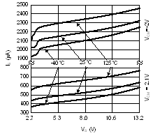
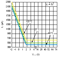
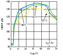
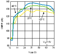
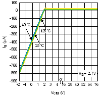
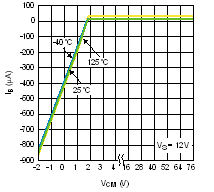
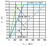
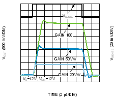
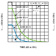
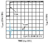
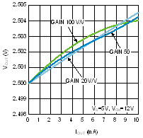
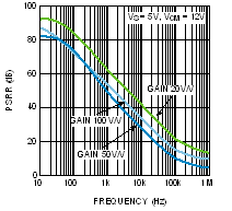
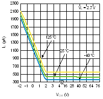
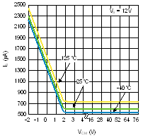
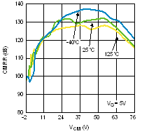
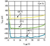
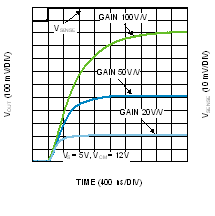
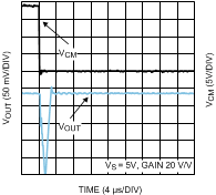
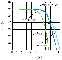
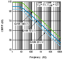
7.9 Typical Characteristics
Unless otherwise specified: TA = 25°C, VS=V+-V-, VSENSE= +IN - (-IN), RL = 10 MΩ.