SNOSB28G August 2010 – November 2014 LMP8640 , LMP8640-Q1 , LMP8640HV
PRODUCTION DATA.
- 1 Features
- 2 Applications
- 3 Description
- 4 Revision History
- 5 Device Comparison Table
- 6 Pin Configuration and Functions
-
7 Specifications
- 7.1 Absolute Maximum Ratings
- 7.2 Handling Ratings - LMP8640, LMP8640HV
- 7.3 Handling Ratings - LMP8640-Q1
- 7.4 Recommended Operating Conditions
- 7.5 Thermal Information
- 7.6 Electrical Characteristics 2.7 V
- 7.7 Electrical Characteristics 5 V
- 7.8 Electrical Characteristics 12 V
- 7.9 Typical Characteristics
- 8 Detailed Description
- 9 Application and Implementation
- 10Power Supply Recommendations
- 11Layout
- 12Device and Documentation Support
- 13Mechanical, Packaging, and Orderable Information
1 Features
- Typical Values, TA = 25°C
- High Common-Mode Voltage Range
- LMP8640: -2 V to 42 V
- LMP8640-Q1: -2 V to 42 V, AEC-Q100
- LMP8640HV: -2 V to 76 V
- Supply Voltage Range: 2.7 V to 12 V
- Gain Options: 20 V/V; 50 V/V; 100 V/V
- Max Gain Error: 0.25%
- Low Offset Voltage: 900 µV
- Input Bias Current: 13 µA
- PSRR: 85 dB
- CMRR (2.1V to 42V): 103 dB
- Temperature Range: -40°C to 125°C
- 6-Pin Thin SOT-23 Package
2 Applications
- High-Side Current Sense
- Vehicle Current Measurement
- Motor Controls
- Battery Monitoring
- Remote Sensing
- Power Management
3 Description
The LMP8640, LMP8640-Q1 and the LMP8640HV are precision current sense amplifiers that detect small differential voltages across a sense resistor in the presence of high input common mode voltages with a supply voltage range from 2.7 V to 12 V.
The LMP8640 and LMP8640-Q1 accept input signals with common mode voltage range from -2 V to 42 V, while the LMP8640HV accepts input signal with common mode voltage range from -2 V to 76 V. The LMP8640 and LMP8640HV have fixed gain for applications that demand accuracy over temperature. The LMP8640 and LMP8640HV come out with three different fixed gains 20 V/V, 50 V/V, 100 V/V ensuring a gain accuracy as low as 0.25%. The output is buffered in order to provide low output impedance. This high side current sense amplifier is ideal for sensing and monitoring currents in DC or battery powered systems, excellent AC and DC specifications over temperature, and keeps errors in the current sense loop to a minimum. The LMP8640 and LMP8640HV are ideal choice for industrial and consumer applications, while the LMP8640-Q1 is an AEC-Q100 grade 1 qualified version of the LMP8640 for automotive applications. The LMP8640-x is available in SOT-23-6 package.
Device Information(1)
| PART NUMBER | PACKAGE | BODY SIZE (NOM) |
|---|---|---|
| LMP8640 | SOT23 (6) | 2.9 mm x 1.6 mm |
| LMP8640-Q1 | ||
| LMP8640HV |
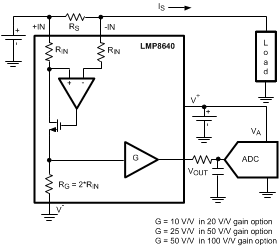
Simplified Schematic
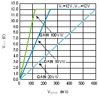
Output Voltage vs Input Voltage