SNOSAK0I December 2004 – January 2015 LMH6550
PRODUCTION DATA.
- 1 Features
- 2 Applications
- 3 Description
- 4 Typical Application Schematic
- 5 Revision History
- 6 Pin Configuration and Functions
- 7 Specifications
- 8 Detailed Description
- 9 Application and Implementation
- 10Power Supply Recommendations
- 11Layout
- 12Device and Documentation Support
- 13Mechanical, Packaging, and Orderable Information
9 Application and Implementation
NOTE
Information in the following applications sections is not part of the TI component specification, and TI does not warrant its accuracy or completeness. TI’s customers are responsible for determining suitability of components for their purposes. Customers should validate and test their design implementation to confirm system functionality.
9.1 Application Information
The LMH6550 is a fully differential amplifier designed to provide low distortion amplification to wide bandwidth differential signals. The LMH6550, though fully integrated for ultimate balance and distortion performance, functionally provides three channels. Two of these channels are the V+ and V− signal path channels, which function similarly to inverting mode operational amplifiers and are the primary signal paths. The third channel is the common-mode feedback circuit. This is the circuit that sets the output common mode as well as driving the V+ and V− outputs to be equal magnitude and opposite phase, even when only one of the two input channels is driven. The common-mode feedback circuit allows single-ended to differential operation.
The LMH6550 is a voltage feedback amplifier with gain set by external resistors. Output common-mode voltage is set by the VCM pin. This pin should be driven by a low impedance reference and should be bypassed to ground with a 0.1-µF ceramic capacitor. Any signal coupling into the VCM will be passed along to the output and will reduce the dynamic range of the amplifier.
The LMH6550 is equipped with a ENABLE pin to reduce power consumption when not in use. The ENABLE pin floats to logic high. If this pin is not used it can be left floating. The amplifier output stage goes into a high impedance state when the amplifier is disabled. The feedback and gain set resistors will then set the impedance of the circuit. For this reason input to output isolation will be poor in the disabled state.
9.2 Typical Applications
9.2.1 Typical Fully Differential Application
The LMH6550 performs best when used with split supplies and in a fully differential configuration. See Figure 21 and Figure 22 for recommend circuits.
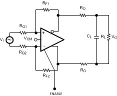 Figure 21. Typical Fully Differential Application Schematic
9.2.1.1 Design Requirements
Applications using fully differential amplifiers have several requirements. The main requirements are high linearity and good signal amplitude. Linearity is accomplished by using well matched feedback and gain set resistors as well as an appropriate supply voltage. The signal amplitude can be tailored by using an appropriate gain. In this design the gain is set for a gain of 2 (RF=500/ RG=250) and the distortion criteria is better than -90 dBc at a frequency of 5 Mhz. The supply voltages are set to +5 V and -5 V and the output common mode is 0 V. The LMH6550 can be placed into shutdown to reduce power dissipation to 10 mW.
9.2.1.2 Detailed Design Procedure
The power supplies for this design are symmetrical ±5-V supplies (not shown for simplicity). The ADC input common mode is 1 V which is within the optimum operating range for the LMH6550 when used on ±5-V split supplies. The gain of this circuit is equal to RF/RG and due to the split supplies can be set to gains of 15 V/V or less. Higher gains will result in values of RF that are too large for high speed operation.
9.2.1.2.1 Fully Differential Operation
The circuit shown in is a typical fully differential application as might be used to drive an ADC. In this circuit closed loop gain, (AV) = VOUT/ VIN = RF/RG. For all the applications in this data sheet VIN is presumed to be the voltage presented to the circuit by the signal source. For differential signals this will be the difference of the signals on each input (which will be double the magnitude of each individual signal), while in single-ended inputs it will just be the driven input signal.
The resistors RO help keep the amplifier stable when presented with a load CL as is typical in an analog to digital converter (ADC). When fed with a differential signal, the LMH6550 provides excellent distortion, balance and common-mode rejection provided the resistors RF, RG and RO are well matched and strict symmetry is observed in board layout. With a DC CMRR of over 80 dB, the DC and low frequency CMRR of most circuits will be dominated by the external resistors and board trace resistance. At higher frequencies board layout symmetry becomes a factor as well. Precision resistors of at least 0.1% accuracy are recommended and careful board layout will also be required.
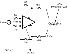 Figure 22. Fully Differential Cable Driver
With up to 15 VPP differential output voltage swing and 80 mA of linear drive current the LMH6550 makes an excellent cable driver as shown in Figure 22. The LMH6550 is also suitable for driving differential cables from a single-ended source.
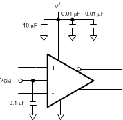
The LMH6550 requires supply bypassing capacitors as shown in Figure 23 and Figure 24. The 0.01 µF and 0.1 µF capacitors should be leadless SMT ceramic capacitors and should be no more than 3 mm from the supply pins. The SMT capacitors should be connected directly to a ground plane. Thin traces or small vias will reduce the effectiveness of bypass capacitors. Also shown in both figures is a capacitor from the VCM pin to ground. The VCM pin is a high impedance input to a buffer which sets the output common-mode voltage. Any noise on this input is transferred directly to the output. Output common-mode noise will result in loss of dynamic range, degraded CMRR, degraded Balance and higher distortion. The VCM pin should be bypassed even if the pin in not used. There is an internal resistive divider on chip to set the output common-mode voltage to the mid point of the supply pins. The impedance looking into this pin is approximately 25 kΩ. If a different output common-mode voltage is desired drive this pin with a clean, accurate voltage reference.
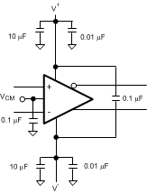 Figure 23. Split Supply Bypassing Capacitors
9.2.1.2.2 Capacitive Drive
As noted in Driving Analog-to-Digital Converters, capacitive loads should be isolated from the amplifier output with small valued resistors. This is particularly the case when the load has a resistive component that is 500 Ω or higher. A typical ADC has capacitive components of around 10 pF and the resistive component could be 1000 Ω or higher. If driving a transmission line, such as 50-Ω coaxial or 100-Ω twisted pair, using matching resistors will be sufficient to isolate any subsequent capacitance. For other applications see Figure 6 and Figure 25 in Typical Characteristics.
9.2.1.2.3 Application Curves
Many application circuits have capacitive loading. As shown in Figure 25, amplifier bandwidth is reduced with increasing capacitive load, so parasitic capacitance should be strictly limited.
To ensure stability, resistance should be added between the capacitive load and the amplifier output pins. The value of the resistor is dependent on the amount of capacitive load as shown in Figure 26. This resistive value is a suggestion. System testing will be required to determine the optimal value. Using a smaller resistor will retain more system bandwidth at the expense of overshoot and ringing, while larger values of resistance will reduce overshoot but will also reduce system bandwidth.
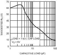 Figure 25. Suggested ROUT vs Cap Load
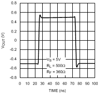 Figure 26. 1 VPP Pulse Response Single-Ended Input
9.2.2 Driving Analog-to-Digital Converters
Analog-to-digital converters (ADC) present challenging load conditions. They typically have high-impedance inputs with large and often variable capacitive components. As well, there are usually current spikes associated with switched capacitor or sample and hold circuits. Figure 27 shows a typical circuit for driving an ADC. The two 56-Ω resistors serve to isolate the capacitive loading of the ADC from the amplifier and ensure stability. In addition, the resistors form part of a low pass filter which helps to provide anti alias and noise reduction functions. The two 39-pF capacitors help to smooth the current spikes associated with the internal switching circuits of the ADC and also are a key component in the low pass filtering of the ADC input. In the circuit of Figure 27 the cutoff frequency of the filter is 1/ (2*π*56 Ω *(39 pF + 14 pF)) = 53 MHz (which is slightly less than the sampling frequency). Note that the ADC input capacitance must be factored into the frequency response of the input filter, and that being a differential input the effective input capacitance is double. Also as shown in Figure 27 the input capacitance to many ADCs is variable based on the clock cycle. See the data sheet for your particular ADC for details.
The amplifier and ADC should be located as closely together as possible. Both devices require that the filter components be in close proximity to them. The amplifier needs to have minimal parasitic loading on the output traces and the ADC is sensitive to high frequency noise that may couple in on its input lines. Some high performance ADCs have an input stage that has a bandwidth of several times its sample rate. The sampling process results in all input signals presented to the input stage mixing down into the Nyquist range (DC to Fs/2). See AN-236 for more details on the subsampling process and the requirements this imposes on the filtering necessary in your system.
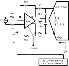 Figure 27. Driving an ADC
9.2.3 Single-Ended Input to Differential Output
The LMH6550 provides excellent performance as an active balun transformer. Figure 28 shows a typical application where an LMH6550 is used to produce a differential signal from a single-ended source.
In single-ended input operation the output common-mode voltage is set by the VCM pin as in fully differential mode. Also, in this mode the common-mode feedback circuit must recreate the signal that is not present on the unused differential input pin. Figure 19 is the measurement of the effectiveness of this process. The common-mode feedback circuit is responsible for ensuring balanced output with a single-ended input. Balance error is defined as the amount of input signal that couples into the output common mode. It is measured as a the undesired output common-mode swing divided by the signal on the input. Balance error can be caused by either a channel to channel gain error, or phase error. Either condition will produce a common-mode shift. Figure 19 measures the balance error with a single-ended input as that is the most demanding mode of operation for the amplifier.
Supply and VCM pin bypassing are also critical in this mode of operation. See the above section on for bypassing recommendations and also see Figure 23 and Figure 24 for recommended supply bypassing configurations.
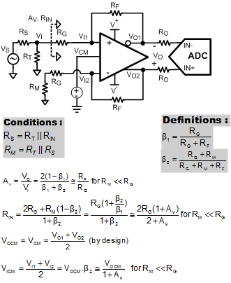 Figure 28. Single-Ended Input to Differential Output Schematic
9.2.4 Single Supply Operation
The input stage of the LMH6550 has a built in offset of 0.7 V towards the lower supply to accommodate single supply operation with single-ended inputs. As shown in Figure 28, the input common-mode voltage is less than the output common voltage. It is set by current flowing through the feedback network from the device output. The input common-mode range of 0.4 V to 3.2 V places constraints on gain settings. Possible solutions to this limitation include AC coupling the input signal, using split power supplies and limiting stage gain. AC coupling with single supply is shown in Figure 29.
In Figure 28 closed loop gain = VO / VI ≊ RF / RG, where VI =VS / 2, as long as RM << RG. Note that in single-ended to differential operation VI is measured single-ended while VO is measured differentially. This means that gain is really 1/2 or 6 dB less when measured on either of the output pins separately. Additionally, note that the input signal at RT (labeled as VI) is 1/2 of VS when RT is chosen to match RS to RIN.
VICM = Input common-mode voltage = (VI1+VI2) / 2.
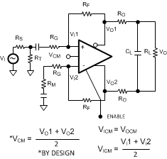 Figure 29. AC-Coupled for Single Supply Operation
9.2.5 Using Transformers
Transformers are useful for impedance transformation as well as for single to differential, and differential to single-ended conversion. A transformer can be used to step up the output voltage of the amplifier to drive very high impedance loads as shown in Figure 30. Figure 32 shows the opposite case where the output voltage is stepped down to drive a low-impedance load.
Transformers have limitations that must be considered before choosing to use one. Compared to a differential amplifier, the most serious limitations of a transformer are the inability to pass DC and balance error (which causes distortion and gain errors). For most applications the LMH6550 will have adequate output swing and drive current and a transformer will not be desirable. Transformers are used primarily to interface differential circuits to 50-Ω single-ended test equipment to simplify diagnostic testing.
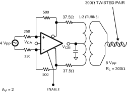 Figure 30. Transformer Out High-Impedance Load
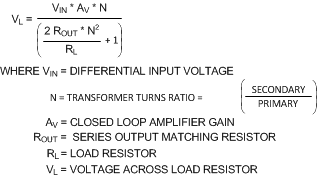 Figure 31. Calculating Transformer Circuit Net Gain
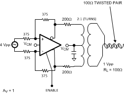 Figure 32. Transformer Out Low-Impedance Load
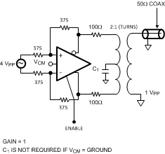 Figure 33. Driving 50-Ω Test Equipment