SNLS270L August 2007 – January 2016 LMH0356
PRODUCTION DATA.
- 1 Features
- 2 Applications
- 3 Description
- 4 Revision History
- 5 Description (continued)
- 6 Pin Configuration and Functions
- 7 Specifications
- 8 Detailed Description
- 9 Application and Implementation
- 10Power Supply Recommendations
- 11Layout
- 12Device and Documentation Support
- 13Mechanical, Packaging, and Orderable Information
封装选项
机械数据 (封装 | 引脚)
散热焊盘机械数据 (封装 | 引脚)
订购信息
9 Application and Implementation
NOTE
Information in the following applications sections is not part of the TI component specification, and TI does not warrant its accuracy or completeness. TI’s customers are responsible for determining suitability of components for their purposes. Customers should validate and test their design implementation to confirm system functionality.
9.1 Application Information
The LMH0356 3-Gbps HD/SD SDI Reclocker with 4:1 Input Mux and FR4 EQs is used in many types of digital video signal processing equipment.
9.2 Typical Application
Figure 4 and Figure 5 show typical system and application circuits for the 48-pin WQFN version of the LMH0356.
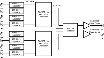 Figure 4. System Block Diagram
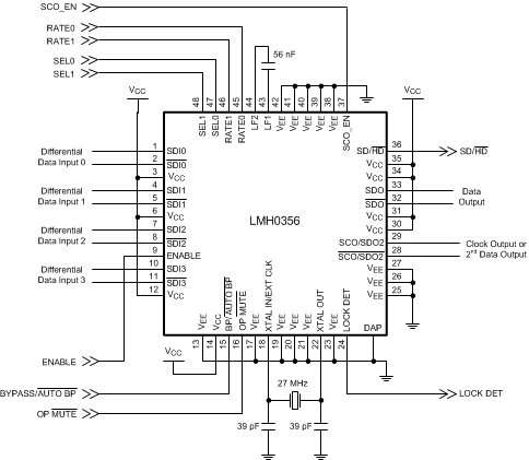 Figure 5. Application Circuit
ENABLE has an internal pullup to enable the device by default. This pin may be pulled low to put the LMH0356 into a powered down mode.
BP/AUTO BP has an internal pulldown to enable Auto Bypass mode by default. This pin may be pulled high to force the LMH0356 to bypass all data.
OP MUTE has an internal pullup to enable the outputs by default. This pin may be pulled low to mute the outputs.
The XTAL IN/EXT CLK and XTAL OUT pins are shown with a 27-MHz crystal and the proper loading. The crystal should match the parameters described in Table 4. Alternately, a 27-MHz LVCMOS compatible clock signal may be input to XTAL IN/EXT CLK.
The active high LOCK DET output provides an indication that proper data is being received and the PLL is locked.
The SD/HD output may be used to drive the SD/HD pin of an SDI cable driver (such as the LMH0302) in order to properly set the cable driver’s edge rate for SMPTE compliance. It defaults to HD/3G (low) when the LMH0356 is not locked.
SCO_EN has an internal pulldown to set the second output (SCO/SDO2) to output data. This pin may be pulled high to set the second output as a serial clock.
The external loop filter capacitor (between LF1 and LF2) must be 56 nF. This is the only supported value; the loop filter capacitor must not be changed.
RATE0 and RATE1 have internal pulldowns to select Auto-Rate Detect mode by default. These pins may also be used to set the device to SD mode or HD/3G mode.
SEL0 and SEL1 have internal pulldowns to select the SDI0 input by default.
9.2.1 Design Requirements
For this design example, use the parameters listed in Table 5 as the input parameters.
Table 5. LMH0356 Design Parameters
| DESIGN PARAMETER | REQUIREMENTS |
|---|---|
| Input AC-coupling capacitors | The user should check output common mode voltage of the device attached to SDI pins. If AC-coupling capacitor is required, AC-coupling capacitor is expected to be 4.7 μF ±10%. Refer to Input Output Interfacing for details. |
| Output AC-coupling capacitors | The user should check input common mode voltage of the device attached to SDO pins. If AC-coupling capacitor is required, AC-coupling capacitor is expected to be 4.7 μF ±10%. Refer to Input Output Interfacing for details. |
| DC power supply coupling capacitors | De-coupling capacitors are required to minimize power supply ripple noise. Place 4.7-μF and 0.1-μF surface mount ceramic capacitors as close to the device VCC pin as possible . |
| High-speed SDI and SDO trace impedance | SDI± and SDO± must be routed with coupled board traces with 100-Ω ± 5% differential impedance. |
| Use of ENABLE, RATE0/1, SCO_EN, OP MUTE, and BP/AUTO BP pins | Set these pins for desired operating mode. |
| LOCK DET pin | Use this pin for lock indication or to OP MUTE pin to enable output when locked. |
| SD/HD Pin | Use SD/HD to set cable driver edge rate or to FPGA for lock rate monitoring. |
9.2.2 Detailed Design Procedure
To begin the design process, determine the following:
- Check that the power supply meets the DC and AC requirements in DC Electrical Characteristics.
- Select the proper pull-high or pull-low resistors for ENABLE, RATE0/1, SCO_EN, OP MUTE, and BP/AUTO BP pins.
- Use SD/HD output signal to set the cable driver edge rate.
- Refer to Input Output Interfacing for Input or Output DC- or AC-coupling.
- Choose small 0402 surface mount ceramic capacitors for AC-coupling and bypass capacitors.
- Pay close attention to high speed printed circuit board layout for the high speed SDI± and SDO± signals.
- Plan out overall system jitter budget with AC Electrical Characteristics in mind.
9.2.2.1 Input Output Interfacing
The inputs are LVPECL compatible. The LMH0356 has a wide input common mode range, and in most cases the input should be DC-coupled. For DC-coupling, the inputs must be kept within the common mode range specified in DC Electrical Characteristics.
Figure 6 shows an example of a DC-coupled interface between the LMH0344 cable equalizer and the LMH0356. The LMH0344 output common mode voltage and voltage swing are within the range of the input common mode voltage and voltage swing of the LMH0356. In this figure, the LMH0344 cable equalizer restores the signal after the coaxial cable. The LMH0356 FR4 equalizer restores the signal after the loss due to the FR4 trace. The LMH0356 inputs have 50-Ω internal terminations (100-Ω differential) to terminate the transmission line, so no additional components are required.
The outputs are LVPECL compatible. SDO is the primary data output and SCO/SDO2 is a second output that may be set as the serial clock or a second data output. Both outputs are always active. The LMH0356 output should be DC-coupled to the input of the receiving device as long as the common mode ranges of both devices are compatible.
Figure 7 shows an example of a DC-coupled interface between the LMH0356 and LMH0302 cable driver. All that is required is a 100-Ω differential termination as shown. The resistor should be placed as close to the LMH0302 input as possible. If desired, this network may be terminated with two 50-Ω resistors and a center tap capacitor to ground in place of the single 100-Ω resistor.
The LMH0356 has multiple ground connections, however; the primary ground connection is through the large exposed DAP. The DAP must be connected to ground for proper operation of the LMH0356.
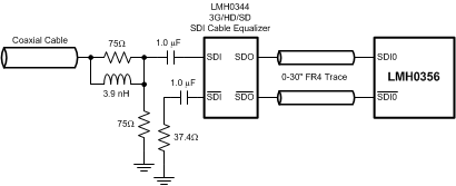 Figure 6. DC Input Interface
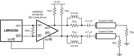 Figure 7. DC Output Interface
9.2.3 Application Curves
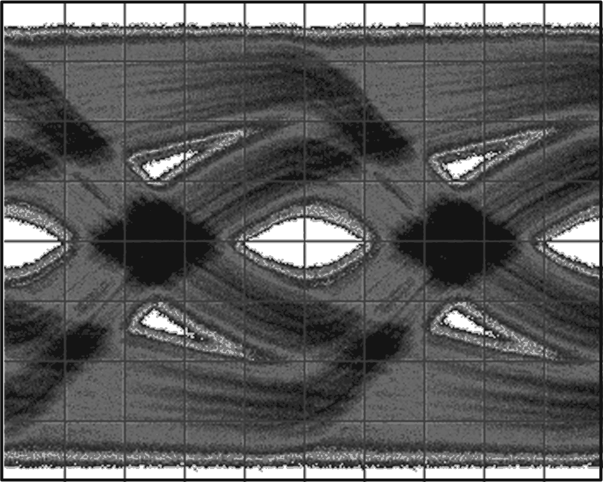 Figure 8. 2.97-Gbps Signal Before FR4 Equalization
 (0.6-UI Jitter)
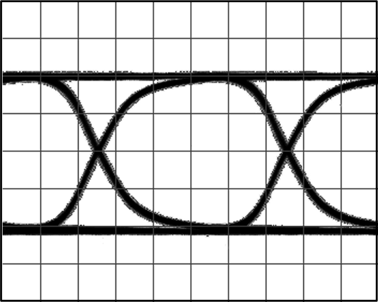 Figure 10. 2.97-Gbps Signal After Reclocking
 (0.06-UI Jitter)
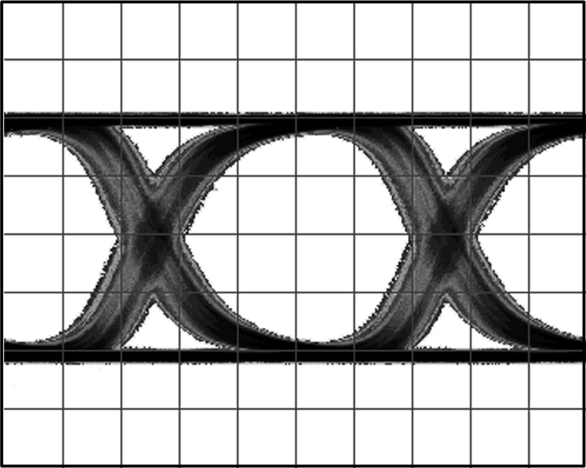 Figure 9. 2.97-Gbps Signal After FR4 Equalization
 (0.23-UI Jitter)