SNLS285H April 2008 – May 2016 LMH0303
PRODUCTION DATA.
- 1 Features
- 2 Applications
- 3 Description
- 4 Revision History
- 5 Pin Configuration and Functions
- 6 Specifications
- 7 Detailed Description
- 8 Application and Implementation
- 9 Power Supply Recommendations
- 10Layout
- 11Device and Documentation Support
- 12Mechanical, Packaging, and Orderable Information
8 Application and Implementation
NOTE
Information in the following applications sections is not part of the TI component specification, and TI does not warrant its accuracy or completeness. TI’s customers are responsible for determining suitability of components for their purposes. Customers should validate and test their design implementation to confirm system functionality.
8.1 Application Information
The LMH0303 is a single-channel SDI cable driver that supports different application spaces. The following sections describe the typical use cases and common implementation practices.
8.1.1 General Guidance for All Applications
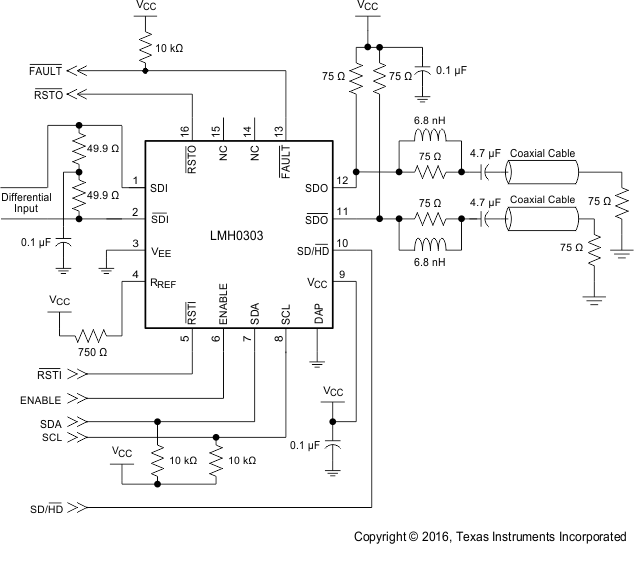
The LMH0303 supports two modes of configuration: Pin control or SMBus mode. Once one of these two control mechanism is chosen, pay attention to the PCB layout for the high-speed signals (see Layout Guidelines). The SMPTE specifications also define the use of AC-coupling capacitors for transporting uncompressed serial data streams with heavy low-frequency content. This specification requires the use of a 4.7-µF AC-coupling capacitor to avoid low frequency DC wander. The 75-Ω signal is also required to meet certain rise and fall timing to facilitate highest eye opening for the receiving device.
SMPTE specifies the requirements for the Serial Digital Interface to transport digital video at SD, HD, 3 Gb/s, and higher data rates over coaxial cables. One of the requirements is meeting the required return loss. This requirement specifies how closely the port resembles 75-Ω impedance across a specified frequency band. Output return loss is dependent on board design. The LMH0303 supports these requirements. To gain additional return loss margin, return loss network in Figure 5 can be optimized.
8.1.2 Cable Fault Detection Operation
The termination fault detection of the LMH0303 indicates when no cable is connected to the output (near end). The termination fault detection works by detecting reflections on the output. The device measures the peak-to-peak output voltage. The output amplitude is normally 800 mVp-p. No termination results in 2x the output voltage (1600 mVp-p) due to the 100% reflection. At the lowest threshold settings, the LMH0303 detects fault even with the amplitude down near 800 mVp-p (perfect termination). At the highest threshold settings, the LMH0303 will detect no fault even as the amplitude approaches 1600 mVp-p (completely unterminated). With the default register settings (HDTFThresh = 9) and with a 3G input, the cable driver will detect the unloaded condition if it sees an amplitude greater than about 450 mVp-p below the maximum (that is, the output amplitude, including the reflection, is about 1.15 Vp-p). Each step of the HD threshold register changes this decision voltage by approximately 100 mV and this can range from 50 to 200 mV. These results are dependent on the board layout and passive components.
Since the termination fault detection threshold is dependent on the PCB layout, the threshold may need to be fine tuned for each design. To help in setting the termination fault threshold, the termination fault counters (registers 0x0A and 0x0B) gauges how the cable driver is interpreting the output termination. The termination fault counter counts the termination faults seen at the LMH0303 output. It counts up or down: up one tick when a termination fault is detected, and down one tick when a proper termination is detected. The counter ranges from 0 to 31 (decimal). When there is no termination fault, the value will be near 0. When the count hits 31, the termination fault indicator is asserted. These registers can be used to fine tune the termination fault threshold setting. If there are many termination fault counts when the output is properly terminated, then the termination fault threshold should be increased. If the register is not showing consistent counts of 31 when the output is unterminated, then the termination fault threshold should be decreased.
8.2 Typical Application
Figure 5 shows the application circuit for the LMH0303.
 Figure 5. Application Circuit
8.2.1 Design Requirements
For the LMH0303 design example, Table 2 lists the design parameters.
Table 2. LMH0303 Design Parameters
| PARAMETER | REQUIREMENT |
|---|---|
| Input termination | Required, 49.9 Ω are recommended (see Figure 5). |
| Output AC-coupling capacitors | Required. Both SDO and SDO require AC-coupling capacitors. SDO AC-coupling capacitors are expected to be 4.7 µF to comply with SMPTE wander requirement. |
| DC power supply coupling capacitors | To minimize power supply noise, place 0.1-µF capacitor as close to the device VCC pin as possible. |
| Distance from device to BNC | Keep this distance as short as possible. |
| High speed SDI and SDI trace impedance | Design differential trace impedance of SDI and SDI with 100 Ω. |
| High speed SDO and SDO trace impedance | Single-ended trace impedance for SDO and SDO with 75 Ω. |
8.2.2 Detailed Design Procedure
The following design procedure is recommended:
- Select a suitable power supply voltage for the LMH0303. It can be powered from a single 3.3-V supply (see Power Supply Recommendations).
- Check that the power supply meets the DC requirements in Recommended Operating Conditions.
- Select the proper pull-high or pull-low for SD/HD to set the slew rate.
- Select proper pull-high or pull-low for ENABLE to enable or disable the output driver.
- Choose a high quality 75-Ω BNC that is capable to support 2.97-Gbps applications. Consult a BNC supplier regarding insertion loss, impedance specifications, and recommended BNC footprint for meeting SMPTE return loss requirements.
- Choose small 0402 surface mount ceramic capacitors for the AC-coupling and bypass capacitors.
- Use proper footprint for BNC and AC-coupling capacitors. Anti-pads are commonly used in power and ground planes under these landing pads to achieve optimum return loss.
8.2.3 Application Curves
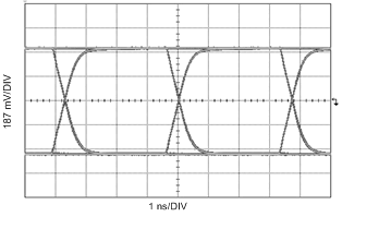
 Figure 6. SDO PRBS10 at 270 Mbps
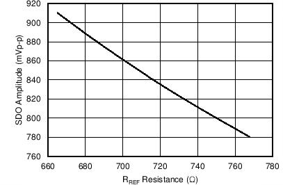
 Figure 7. SDO Amplitude vs RREF Resistance