ZHCSG61B march 2017 – april 2023 LMG1205
PRODUCTION DATA
8.2.2.3 Power Dissipation
The power consumption of the driver is an important measure that determines the maximum achievable operating frequency of the driver. It must be kept below the maximum power dissipation limit of the package at the operating temperature. The total power dissipation of the LMG1205 is the sum of the gate driver losses and the bootstrap diode power loss.
The gate driver losses are incurred by charge and discharge of the capacitive load. It can be approximated as
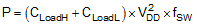
where
- CLoadH and CLoadL are the high-side and the low-side capacitive loads, respectively
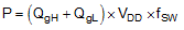
It can also be calculated with the total input gate charge of the high-side and the low-side transistors as
There are some additional losses in the gate drivers due to the internal CMOS stages used to buffer the LO and HO outputs. Figure 8-2 shows the measured gate driver power dissipation versus frequency and load capacitance. At higher frequencies and load capacitance values, the power dissipation is dominated by the power losses driving the output loads and agrees well with the above equations. Figure 8-2 can be used to approximate the power losses due to the gate drivers.

The bootstrap diode power loss is the sum of the forward bias power loss that occurs while charging the bootstrap capacitor and the reverse bias power loss that occurs during reverse recovery. Because each of these events happens once per cycle, the diode power loss is proportional to the operating frequency. Larger capacitive loads require more energy to recharge the bootstrap capacitor resulting in more losses. Higher input voltages (VIN) to the half bridge also result in higher reverse recovery losses.
Figure 8-3 and Figure 8-4 show the forward bias power loss and the reverse bias power loss of the bootstrap diode respectively. The plots are generated based on calculations and lab measurements of the diode reverse time and current under several operating conditions. Figure 8-3 and Figure 8-4 can be used to predict the bootstrap diode power loss under different operating conditions.


The sum of the driver loss and the bootstrap diode loss is the total power loss of the IC. For a given ambient temperature, the maximum allowable power loss of the IC can be defined as Equation 5.
