SNAS425C October 2007 – October 2014 LM98519
PRODUCTION DATA.
- 1 Features
- 2 Applications
- 3 Description
- 4 Revision History
- 5 Pin Configuration and Functions
- 6 Specifications
-
7 Detailed Description
- 7.1 Overview
- 7.2 Functional Block Diagrams
- 7.3 Feature Description
- 7.4 Device Functional Modes
- 7.5 Programming
- 7.6 Register Maps
- 8 Application and Implementation
- 9 Power Supply Recommendations
- 10Layout
- 11Device and Documentation Support
- 12Mechanical, Packaging, and Orderable Information
6 Specifications
6.1 Absolute Maximum Ratings
over operating free-air temperature range (unless otherwise noted) (1)| MIN | MAX | UNIT | ||
|---|---|---|---|---|
| Supply Voltage | –0.3 | 4.2 | V | |
| Voltage at any Pin (except VREG) | –0.3 | VDDD + 0.3 | V | |
| Voltage at VREG Pin | –0.3 | 2.1 | V | |
| Input Current at any Pin(2) | ±25 | mA | ||
| Package Input Current(2) | ±50 | mA | ||
(1) Stresses beyond those listed under Absolute Maximum Ratings may cause permanent damage to the device. These are stress ratings only, which do not imply functional operation of the device at these or any other conditions beyond those indicated under Recommended Operating Conditions. Exposure to absolute-maximum-rated conditions for extended periods may affect device reliability.
(2) When the input voltage (VIN) at any pin exceeds the power supplies [VIN < (GND – 0.3 V) or VIN > (VDDA + 0.3 V)], the DC current at that pin should be limited to ±25 mA. The 50 mA DC maximum package input current means that a maximum of two pins can simultaneously have input currents that equal 25 mA.
6.2 Handling Ratings
| MIN | MAX | UNIT | |||
|---|---|---|---|---|---|
| Tstg | Storage temperature range | –65 | 150 | °C | |
| V(ESD) | Electrostatic discharge(1) | Human body model (HBM), per ANSI/ESDA/JEDEC JS-001(2) | 2500 | V | |
| Human body model (HBM, rated for the following pins only: SHP, SHD, CLPIN, BLKCLP, AGC_ONB, MCLK, RESETB, SENB, SCLK, SDI, SDO).(3) | 7500 | ||||
| Machine model (MM) | 250 | ||||
| Charged device model (CDM), per JEDEC specification JESD22-C101, all pins(4) | 1000 | ||||
(1) Electrostatic discharge (ESD) to measure device sensitivity and immunity to damage caused by assembly line electrostatic discharges in to the device. Human body model, 100 pF discharged through a 1.5 kΩ resistor. Machine model, 200 pF discharged directly into each pin. Charged device model (CDM) simulates a pin slowly acquiring charge (such as from a device sliding down the feeder in an automated assembler) then rapidly being discharged.
(2) Level listed above is the passing level per ANSI, ESDA, and JEDEC JS-001. JEDEC document JEP155 states that 2500-V HBM allows safe manufacturing with a standard ESD control process.
(3) Level listed above is the passing level per ANSI, ESDA, and JEDEC JS-001. JEDEC document JEP155 states that 7500-V HBM allows safe manufacturing with a standard ESD control process
(4) Level listed above is the passing level per EIA-JEDEC JESD22-C101. JEDEC document JEP157 states that 1000-V CDM allows safe manufacturing with a standard ESD control process.
6.3 Recommended Operating Conditions
over operating free-air temperature range (unless otherwise noted)| MIN | NOM | MAX | UNIT | ||
|---|---|---|---|---|---|
| Analog Supply Voltage Range | 3.0 | 3.6 | V | ||
| Digital Supply Voltage Range | 3.0 | 3.6 | V | ||
| Output Supply Voltage Range | 2.25 | VDDD | V | ||
| DC Power Supply Voltage Relationships(1) | VDDD ≥ VDDA, VDDD ≥ VDDO | ||||
| Voltage at any Digital I/O Pin | 0 | VDDD | V | ||
| Voltage at any Analog Input Pin | 0 | VDDA | V | ||
| Voltage at any Data Output Pin | 0 | VDDO | V | ||
| Specified Temperature Range | 0 | 70 | °C | ||
(1) Static voltage levels on VDDD must be at the same voltage or slightly higher than VDDO or VDDA. Therefore, driving all three power supplies from a common linear voltage regulator is recommended. Please see the following diagram. 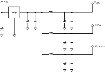
6.4 Thermal Information
| THERMAL METRIC(1) | LM98519 | UNIT | |
|---|---|---|---|
| PFC | |||
| 80 TERMINALS | |||
| RθJA | Junction-to-ambient thermal resistance | 32 | °C/W |
(1) For more information about traditional and new thermal metrics, see the IC Package Thermal Metrics application report, SPRA953.
6.5 Electrical Characteristics
The following specifications apply for VDDA = VDDD = VDDO = 3.3 V; FMCLK = 65 Ms/s and TA =+25°C unless otherwise noted. Boldface limits apply for TA = TMIN to TMAX. All other limits apply for TA =+25°C.| PARAMETER | TEST CONDITIONS | MIN | TYP | MAX | UNIT | |
|---|---|---|---|---|---|---|
| ADC/AFE | ||||||
| Resolution | No missing codes | 10 | bits | |||
| INL | Gain = 1x | –2.4 | –0.75 to 0.9 | 1.95 | lsb | |
| Gain = 6x | –1.85 to 2.0 | |||||
| DNL | Gain = 1x | –0.99 | –0.55 to 0.7 | 1.5 | lsb | |
| Gain = 6x | –0.65 to 0.85 | |||||
| Noise Floor (SNR)(1) | Gain = 1x | 67.5 | dB | |||
| Gain = 6x | 55 | |||||
| Analog Input Range | Peak-to-peak, CDS gain = 1x | 1.12 | 1.19 | 1.29 | V | |
| Peak-to-peak, CDS gain = 2.1x | 0.55 | 0.58 | 0.62 | |||
| Analog Input Leakage (Osx inputs) | GND < Vin < VDDA Source Follower Enabled – OVP off |
–330 | ±25 | 140 | nA | |
| RCLAMP | Input Clamp Impedance | From bench and design | 43 | Ω | ||
| Conversion Ratio | CDS/SH Gain Setting = 1x PGA gain setting = Min (Typical values by design)(2) |
0.78 | 0.85 | 0.92 | lsb/mV | |
| Conversion Ratio Color to Color Error |
0.26% | |||||
| Conversion Ratio Ch1 to Ch2 Error |
0.13% | |||||
| Crosstalk – Color to Color | R1,B1 to G1; R1,G1 to B1, etc. R2, B2, to G2; R2, G2, to B2, etc. Gain = 20x setting |
0.8% | ||||
| Crosstalk – Ch1 to Ch2 | R1 to R2, R2 to R1, G1 to G2, G2 to G1, B1 to B2, B2 to B1 Gain = 20x setting |
0.3% | ||||
| PD | Active Mode Power Consumption | 3.3 V | 1041 | 1271 | mW | |
| IDDA | 3.3 V | 257 | mA | |||
| IDDD | 3.3 V | 58 | mA | |||
| IDDO | 3.3 V | 70 | mA | |||
| PD | Power-Down Mode Power Consumption |
3.3 V – MCLK Active | 153 | 201 | mW | |
| PGA (8 bits) Gain = 283/(283-M) | ||||||
| PGA Gain Range(3) | Max Setting/Min Setting | 19.5 | 20 | 20.9 | dB | |
| PGA Max Stepsize | Largest PGA Step | 0.3 | dB | |||
| PGA Monotonicity | Monotonic | |||||
| PGA Error (Difference from ideal curve) | 1.15% | |||||
| CDS/SH | ||||||
| CDS/SH Gain | Gain at 2x / Gain at 1x | 2 | 2.1 | 2.13 | V/V | |
| OFFSET FDAC (±10 bits) | ||||||
| DAC Full Scale (input referred) | Large FDAC range | 102 | 110.5 | 120 | ±mV | |
| Small FDAC range | 51 | 59.5 | 68 | |||
| DAC Monotonicity | Monotonic | |||||
| OFFSET CDAC (±4 bits) | ||||||
| DAC Full Scale (input referred) | 255 | 277 | 300 | ±mV | ||
| DAC Monotonicity | Monotonic | |||||
| LOGIC I/O DC PARAMETERS | ||||||
| VIH | Logic Input Voltage High SHP, SHD, CLPIN, BLKCLP, AGC_ONB, MCLK, SCLK, SDI, SENB |
2.0 | V | |||
| VIL | Logic Input Voltage Low SHP, SHD, CLPIN, BLKCLP, AGC_ONB, MCLK, SCLK, SDI, SENB |
0.8 | ||||
| IIN | Logic Input Leakage | Excludes AGC_ONB, BLKCLP, SENB, RESETB due to pull-ups or pull-downs on those pins | –100 | 65 | 100 | nA |
| VOH | Logic Output Voltage High | VDDD = 3.6 V, Iout = -0.5 mA | 3.3 | 3.56 | V | |
| VDDD = 3.0 V, Iout = -0.5 mA | 2.7 | 2.9 | ||||
| VOL | Logic Output Voltage Low | VDDD = 3.6 V, Iout = 1.6 mA | 0.11 | 0.2 | V | |
| VDDD = 3.0 V, Iout = 1.6 mA | 0.11 | 0.2 | ||||
| VRES | Power On Reset Threshold | From simulation | 1.18 | 1.5 | V | |
| AFE/ADC TIMING | ||||||
| fMCLK | MCLK frequency | 6 channel mode | 10 | 65 | MHz | |
| 3 channel mode | 10 | 32.5 | ||||
| MCLK Duty Cycle | 45% | 55% | ||||
| Input Sampling Rate | 6 Channel Mode | 5 | 32.5 | MS/s | ||
| 3 Channel Mode | 10 | 32.5 | ||||
| tRESET | RESETB Pulse Width | MCLK Present Mode | 2 | tMCLK | ||
| MCLK Idle Mode | 50 | ns | ||||
| tRESET_CLR | RESETB Clear Time | MCLK Present Mode (ensured by design) | 3 | tMCLK | ||
| MCLK Idle Mode (ensured by design) | 10 | ns | ||||
| tSHD | SHP/SHD high period | Ensured by design | 8.2 | ns | ||
| tMCS_MIN | MCLK high to SAMPLE high (Minimum)(7) | SH3 Mode – ADC Rate MCLK | 9 | 13 | ns(4) | |
| SH2 Mode | 10.5 | 14.5 | ||||
| SH1b Mode | 2.4 | 5 | ||||
| CDSb Mode | 1.8 | 4 | ||||
| tHMC_MIN | HOLD high to MCLK high (Minimum)(7) | SH3 Mode – ADC Rate MCLK | 0.7 | 3.5 | ns(4) | |
| SH2 Mode | –0.7 | 3 | ||||
| SH1b Mode | –2.1 | 2 | ||||
| CDS Mode | –3.1 | 1 | ||||
| tMCH_MIN | MCLK high to HOLD high (Minimum)(7) | SH3 Mode – ADC Rate MCLK | 1 | 5 | ns | |
| tAD | Aperture delay | 4 | 5 | 6.9 | ns | |
| Aperture delay variation | 0.2 | 1 | ||||
| tBCLPINB, tBLKCLP | CLPIN/BLKCLP Pulse Width | (high or low) | 2 | tMCLK | ||
| tIS | CLPIN/BLKCLP Setup | 3 | ns | |||
| tIH | CLPIN/BLKCLP Hold | 3 | ns | |||
| tC_B | CLPIN neg. edge to BLKCLP start | 6 Channel mode | 16 | Pixels | ||
| 3 Channel mode | 10 | |||||
| tLAT(1) | 6 Channel Mode | 6 Channel Mode, ADC Rate MCLK | 11 | tMCLK | ||
| Channel 1 Latency | 6 Channel Mode, Pixel Rate MCLK | 5 | ||||
| tLAT(2) | 6 Channel Mode | 6 Channel Mode, ADC Rate MCLK | 12 | tMCLK | ||
| Channel 2 Latency | 6 Channel Mode, Pixel Rate MCLK | 5.5 | ||||
| tLAT | 3 Channel Mode Latency | 3 Channel Mode ADC=Pixel Rate MCLK | 11 | tMCLK | ||
| tOD | Output Data Delay | Pixel Rate MCLK: | ns(5) | |||
| 6 Channel Mode – Channel 1 | 2 | 5.2 | 8 | |||
| 6 Channel Mode – Channel 2 | 2 | 5 | 8 | |||
| ADC Rate MCLK: | ns | |||||
| 6 Channel Mode – Channel 1 | 3 | 6 | 9 | |||
| 6 Channel Mode – Channel 2 | 3 | 6 | 9 | |||
| 3 Channel Mode | 2 | 5.4 | 9 | |||
(1) SNR = 20log(1024/Output Noise(lsb rms)) with input = DC
(2) For conversion ratio min/max, variation and error, Conversion ratio is: (Digital Max – Digital Min)/(Vin Max – Vin Min). Measured at gain setting of 1x
(3) PGA gain range is: [(ADC_OUT(PGA at 1111111111)) / (ADC_OUT(PGA at 0000000000))]
(4) Measured with AFEPHASE = 11. For other AFEPHASE settings,these sample input timings will shift earlier with respect to MCLK as follows. (tHMC will increase by these amounts, tMCH will decrease by these amounts):
- AFEPHASE = 10 – Earlier by ¼ pixel period
- AFEPHASE = 01 – Earlier by ½ pixel period
- AFEPHASE = 00 – Earlier by ¾ pixel period
(5) In Pixel Rate MCLK mode, the output data delay for Channel 2 data may be different under certain conditions of low MCLK duty cycle (< 50%). In that case the approximate output data delay tOD will increase by the following: (50 – MCLK Duty Cycle Percent)/100 * TMCLK
(6) SENB high pulse width should be > 50 ns when MCLK is not supplied. It should be > 5 MCLK when MCLK_ALIVE bit is set to 1 and MCLK is supplied.
(7) Refer to Sampling Timing Diagrams
6.6 Serial Interface Timing
| MIN | TYP | MAX | UNIT | ||
|---|---|---|---|---|---|
| tCP | SCLK period | 50 | ns | ||
| tWH | SCLK High width | 20 | ns | ||
| tWL | SCLK Low width | 20 | ns | ||
| tIS | SDI Setup time | 5 | ns | ||
| tIH | SDI Hold time | 5 | ns | ||
| tSENSC | SENB low before SCLK rising | 5 | ns | ||
| tSCSEN | SENB high after SCLK rising | 5 | ns | ||
| tSENW | SENB high width(6) | 50 | ns | ||
| 5 | tMCLK | ||||
| tOD | SDO Output delay | 2 | 10 | ns | |
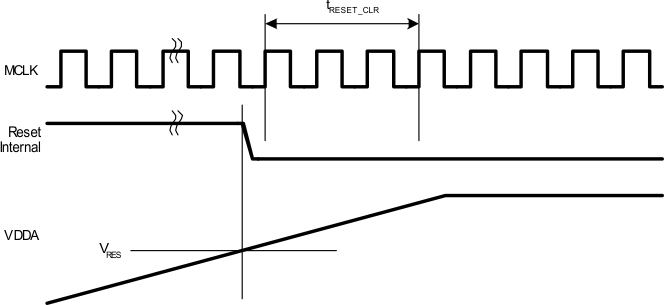 Figure 1. POR - Power On Reset
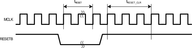 Figure 2. RESETB Input Timing
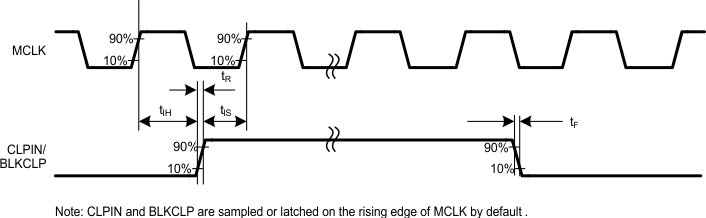 Figure 3. Input Setup and Hold Timing
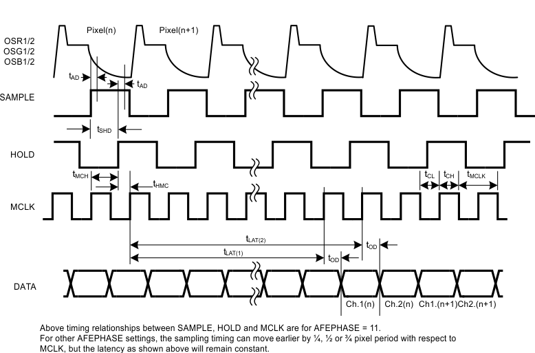 Figure 4. Output Latency and Timing – 6 Channel Mode – ADC Rate MCLK
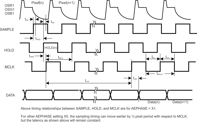 Figure 6. Output Latency and Timing – 3 Channel Mode
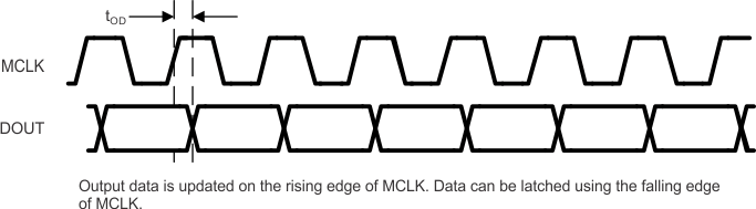 Figure 7. Data Capture Timing – 6 Channel – ADC Rate MCLK
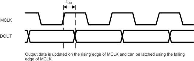 Figure 9. Data Capture Timing – 3 Channel