SNVS233C March 2003 – December 2015 LM8365
PRODUCTION DATA.
7 Detailed Description
7.1 Overview
The LM8365 ultra-low current voltage detector was designed to monitor voltages and to provide an indication when the monitored voltage, VIN, dropped below a precisely trimmed threshold voltage. The voltage detector of the LM8365 drives a time delay generator that may be programmed for fixed lengths of time depending on the application needs. This characteristic is displayed in the typical operating timing diagram in Figure 1.
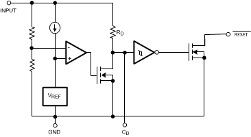
7.2 Functional Block Diagram
 Figure 13. Open-Drain Output
7.3 Feature Description
VIN is the voltage that is being monitored and as it decreases passed the precisely trimmed threshold VDET−, the Active Low RESET output drops to a Logic Low state and the CD pin drops to 0 V. During this state the external capacitor connected to the CD pin is immediately discharged by an internal N-Channel MOSFET. When VIN increases above the threshold VDET+ (VDET− + VHYS) the capacitor connected to the CD pin starts to charge up to VIN through an internal pullup resistor RD. Once the capacitor has charged up past the internal Delay Pin Threshold, which is typically 0.675 VIN, the RESET output will revert back to it's original state. The LM8365 have built-in hysteresis to help prevent erratic reset operation when the input voltage crosses the threshold.
The LM8365 has a wide variety of applications that can take advantage of its precision and low current consumption to monitor Input voltages even though it was designed as a reset controller in portable microprocessor based systems. It is a very cost-effective and space-saving device that will protect your more expensive investments of microprocessors and other devices that need a specified supply voltage and time delay for proper operation.
The propagation delay time for the LM8365 is measured using a 470-kΩ pullup resistor connected to from the RESET output pin to 5 V in addition to a 10-pF capacitive load connected from the same pin to GND. Figure 2 shows the timing diagram for the measurement for the propagation delay. VDET+ is equal to the sum of the detector threshold, VDET−, and the built in hysteresis, VHYS. tD1 is the propagation time from High-to-Low and tD2 is the propagation from Low-to-High.
7.4 Device Functional Modes
7.4.1 Reset Output Low
When VIN decreases below the precisely trimmed threshold VDET−, the CD pin voltage will drop to 0 V and the Reset pin will output low.
7.4.2 Reset Output High
When VIN increases above the precisely trimmed threshold VDET+ (VDET− + VHYS), the capacitor connected to the CD pin starts to charge up to VIN through an internal pull-up resistor RD. Once the capacitor has charged up past the internal Delay Pin Threshold, which is typically 0.675 VIN, the RESET output will be pulled high, assuming an external pullup resistor is connected from Reset to VIN.