ZHCSFV1 December   2016 LM73-Q1

PRODUCTION DATA.  

  1. 特性
  2. 应用
  3. 说明
  4. 修订历史记录
  5. Pin Configuration and Functions
  6. Specifications
    1. 6.1 Absolute Maximum Ratings
    2. 6.2 ESD Ratings
    3. 6.3 Recommended Operating Conditions
    4. 6.4 Thermal Information
    5. 6.5 Temperature-to-Digital Converter Characteristics
    6. 6.6 Logic Electrical Characteristics- Digital DC Characteristics
    7. 6.7 SMBus Digital Switching Characteristics
    8. 6.8 Typical Characteristics
  7. Detailed Description
    1. 7.1 Overview
    2. 7.2 Functional Block Diagram
    3. 7.3 Feature Description
      1. 7.3.1 Power-On Reset
      2. 7.3.2 One-Shot Conversion
      3. 7.3.3 Temperature Data Format
      4. 7.3.4 SMBus Interface
      5. 7.3.5 ALERT Function
      6. 7.3.6 Communicating With the LM73-Q1
        1. 7.3.6.1 Reading from the LM73-Q1
        2. 7.3.6.2 Writing to the LM73-Q1
    4. 7.4 Device Functional Modes
      1. 7.4.1 Shutdown Mode
    5. 7.5 Register Map
      1. 7.5.1 LM73-Q1 Registers
        1. 7.5.1.1 Pointer Register
        2. 7.5.1.2 Temperature Data Register
        3. 7.5.1.3 Configuration Register
        4. 7.5.1.4 THIGH Upper-Limit Register
        5. 7.5.1.5 TLOW Lower-Limit Register
        6. 7.5.1.6 Control/Status Register
        7. 7.5.1.7 Identification Register
  8. Application and Implementation
    1. 8.1 Application Information
      1. 8.1.1 Thermal Path Considerations
      2. 8.1.2 Output Considerations: Tight Accuracy, Resolution and Low Noise
    2. 8.2 Typical Application
      1. 8.2.1 Design Requirements
      2. 8.2.2 Detailed Design Procedure
      3. 8.2.3 Application Curve
  9. Power Supply Recommendations
  10. 10Layout
    1. 10.1 Layout Guidelines
    2. 10.2 Layout Example
  11. 11器件和文档支持
    1. 11.1 相关文档 
    2. 11.2 接收文档更新通知
    3. 11.3 社区资源
    4. 11.4 商标
    5. 11.5 静电放电警告
    6. 11.6 Glossary
  12. 12机械、封装和可订购信息

封装选项

机械数据 (封装 | 引脚)
散热焊盘机械数据 (封装 | 引脚)
订购信息

Pin Configuration and Functions

DDC Package
6-Pin (SOT-23)
Top View
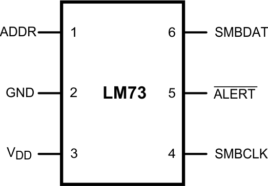
LM73-Q1 20147802.gif

Pin Functions

PIN TYPE EQUIVALENT CIRCUIT FUNCTION
NO. NAME
1 ADDR CMOS Logic
Input
(three levels)
LM73-Q1 20147806.gif
Address Select Input: One of three device addresses is selected by connecting to ground, left floating, or connecting to VDD.
2 GND Ground Ground
3 VDD Power Supply Voltage
4 SMBCLK CMOS Logic
Input
LM73-Q1 20147805.gif
Serial Clock: SMBus clock signal. Operates up to 400 kHz. Low-pass filtered.
5 ALERT Open-Drain Output
LM73-Q1 20147804.gif
Digital output which goes active whenever the measured temperature exceeds a programmable temperature limit.
6 SMBDAT Open-Drain
Input/Output
LM73-Q1 20147805.gif
Serial Data: SMBus bi-directional data signal used to transfer serial data synchronous to the SMBCLK. Low-pass filtered.