ZHCSFV3 November 2016 LM53602 , LM53603
PRODUCTION DATA.
- 1 特性
- 2 应用
- 3 说明
- 4 修订历史记录
- 5 Device Comparison Table
- 6 Pin Configuration and Functions
- 7 Specifications
- 8 Detailed Description
- 9 Application and Implementation
- 10Power Supply Recommendations
- 11Layout
- 12器件和文档支持
- 13机械、封装和可订购信息
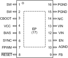
6 Pin Configuration and Functions
PWP Package
16-Lead HTSSOP
Top View

Pin Functions
| PIN | I/O(1) | DESCRIPTION | |
|---|---|---|---|
| NO. | NAME | ||
| 1, 2 | SW | P | Regulator switch node. Connect to power inductor. Connect pins 1 and 2 directly together at the PCB. |
| 3 | CBOOT | P | Bootstrap supply input for gate drivers. Connect a high-quality, 470-nF capacitor from this pin to SW. |
| 4 | VCC | O | Internal 3.15-V regulator output. Used as supply to internal control circuits. Do not connect to any external loads. Can be used as logic supply for control inputs. Connect a high-quality, 3.3-µF capacitor from this pin to GND. |
| 5 | BIAS | P | Input to internal voltage regulator. Connect to output voltage point. Do not ground. Connect a high-quality, 0.1-µF capacitor from this pin to GND. |
| 6 | SYNC | I | Synchronization input to regulator. Used to synchronize the regulator switching frequency to the system clock. When not used connect to GND; do not float. |
| 7 | FPWM | I | Mode control input to regulator. High = forced PWM (FPWM). Low = auto mode; automatic transition between PFM and PWM. Do not float. |
| 8 | RESET | O | Open-drain reset output. Connect to suitable voltage supply through a current limiting resistor. High = power OK. Low = fault. RESET goes low when EN = low. |
| 9 | FB | I | Feedback input to regulator. Connect to output voltage sense point for fixed 5-V and 3.3-V output. Connect to feedback divider tap point for ADJ option. Do not float or ground. |
| 10 | AGND | G | Analog ground for regulator and system. All electrical parameters are measured with respect to this pin. Connect to EP and PGND on PCB. |
| 11 | EN | I | Enable input to the regulator. High = ON. Low = OFF. Can be connected directly to VIN. Do not float. |
| 12, 13 | VIN | P | Input supply to the regulator. Connect a high-quality bypass capacitor(s) from this pin to PGND. Connect pins 12 and 13 directly together at the PCB. |
| 14 | N/C | — | This pin has no connection to the device. |
| 15, 16 | PGND | G | Power ground to internal low-side MOSFET. Connect to AGND and system ground. Connect pins 15 and 16 directly together at the PCB. |
| 17 | EP | G | Exposed die attach paddle. Connect to ground plane for adequate heat sinking and noise reduction. |
(1) O = Output, I = Input, G = Ground, P = Power