ZHCSIN4B August   2018  – June 2021 LM5146-Q1

PRODUCTION DATA  

  1. 特性
  2. 应用
  3. 说明
  4. Revision History
  5. 说明(续)
  6. Pin Configuration and Functions
    1. 6.1 Wettable Flanks
  7. Specifications
    1. 7.1 Absolute Maximum Ratings
    2. 7.2 ESD Ratings 
    3. 7.3 Recommended Operating Conditions
    4. 7.4 Thermal Information
    5. 7.5 Electrical Characteristics
    6. 7.6 Switching Characteristics
    7. 7.7 Typical Characteristics
  8. Detailed Description
    1. 8.1 Overview
    2. 8.2 Functional Block Diagram
    3. 8.3 Feature Description
      1. 8.3.1  Input Range (VIN)
      2. 8.3.2  Output Voltage Setpoint and Accuracy (FB)
      3. 8.3.3  High-Voltage Bias Supply Regulator (VCC)
      4. 8.3.4  Precision Enable (EN/UVLO)
      5. 8.3.5  Power Good Monitor (PGOOD)
      6. 8.3.6  Switching Frequency (RT, SYNCIN)
        1. 8.3.6.1 Frequency Adjust
        2. 8.3.6.2 Clock Synchronization
      7. 8.3.7  Configurable Soft Start (SS/TRK)
        1. 8.3.7.1 Tracking
      8. 8.3.8  Voltage-Mode Control (COMP)
      9. 8.3.9  Gate Drivers (LO, HO)
      10. 8.3.10 Current Sensing and Overcurrent Protection (ILIM)
      11. 8.3.11 OCP Duty Cycle Limiter
    4. 8.4 Device Functional Modes
      1. 8.4.1 Shutdown Mode
      2. 8.4.2 Standby Mode
      3. 8.4.3 Active Mode
      4. 8.4.4 Diode Emulation Mode
      5. 8.4.5 Thermal Shutdown
  9. Application and Implementation
    1. 9.1 Application Information
      1. 9.1.1 Design and Implementation
      2. 9.1.2 Power Train Components
        1. 9.1.2.1 Inductor
        2. 9.1.2.2 Output Capacitors
        3. 9.1.2.3 Input Capacitors
        4. 9.1.2.4 Power MOSFETs
      3. 9.1.3 Control Loop Compensation
      4. 9.1.4 EMI Filter Design
    2. 9.2 Typical Applications
      1. 9.2.1 Design 1 – 12-A High-Efficiency Synchronous Buck DC/DC Regulator for Automotive Applications
        1. 9.2.1.1 Design Requirements
        2. 9.2.1.2 Detailed Design Procedure
        3. 9.2.1.3 Custom Design With WEBENCH® Tools
        4. 9.2.1.4 Custom Design With Excel Quickstart Tool
        5. 9.2.1.5 Application Curves
      2. 9.2.2 Design 2 – High Density, 12-V, 8-A Rail From 48-V Automotive Battery Power
        1. 9.2.2.1 Design Requirements
        2. 9.2.2.2 Detailed Design Procedure
        3. 9.2.2.3 Application Curves
  10. 10Power Supply Recommendations
  11. 11Layout
    1. 11.1 Layout Guidelines
      1. 11.1.1 Power Stage Layout
      2. 11.1.2 Gate Drive Layout
      3. 11.1.3 PWM Controller Layout
      4. 11.1.4 Thermal Design and Layout
      5. 11.1.5 Ground Plane Design
    2. 11.2 Layout Example
  12. 12Device and Documentation Support
    1. 12.1 Device Support
      1. 12.1.1 第三方产品免责声明
      2. 12.1.2 Development Support
        1. 12.1.2.1 Custom Design With WEBENCH® Tools
    2. 12.2 Documentation Support
      1. 12.2.1 Related Documentation
        1. 12.2.1.1 PCB Layout Resources
        2. 12.2.1.2 Thermal Design Resources
    3. 12.3 接收文档更新通知
    4. 12.4 支持资源
    5. 12.5 Trademarks
    6. 12.6 Electrostatic Discharge Caution
    7. 12.7 Glossary
  13. 13Mechanical, Packaging, and Orderable Information

封装选项

请参考 PDF 数据表获取器件具体的封装图。

机械数据 (封装 | 引脚)
  • RGY|20
散热焊盘机械数据 (封装 | 引脚)
订购信息

Typical Characteristics

VVIN = 48 V, RRT = 25 kΩ, SYNCIN tied to VCC, EN/UVLO tied to VIN (unless otherwise noted).
GUID-70B26539-6F63-4410-A41F-AF2988F96223-low.gif
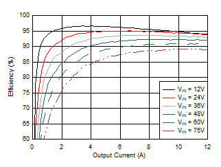
VOUT = 5 V FSW = 300 kHz
See Figure 9-5 RRT = 33.2 kΩ
Figure 7-1 Efficiency vs Load, CCM
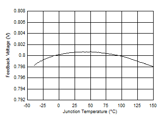
GUID-D1C00024-083A-4220-B12A-1B9AFBCEEE38-low.gifFigure 7-3 FB Voltage vs Junction Temperature
GUID-6C59053E-2D75-4CAB-BABB-56E4A017A461-low.gif
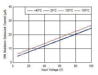
VSW = 0 V VEN/UVLO = 0 V
Figure 7-5 IQ-SHD vs Input Voltage
GUID-5AE33E7C-51F9-4BBC-A5A6-5543F8E40E6D-low.gif
VSW = 0 V VEN/UVLO = VVIN VSS/TRK = 0 V
Figure 7-7 IQ-OPERATING (Nonswitching) vs Input Voltage
GUID-CA8C0823-B8B9-4D18-A5A1-963A8F89F893-low.gif
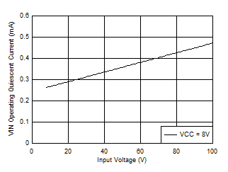
VSW = 0 V VVCC = VBST = VILIM VFB = 0 V
Figure 7-9 VIN Quiescent Current with External VCC Applied
GUID-F493D335-D721-47B1-AEED-BB72642689AD-low.gif
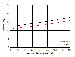
VSW = 0 V
Figure 7-11 Deadtime vs Junction Temperature
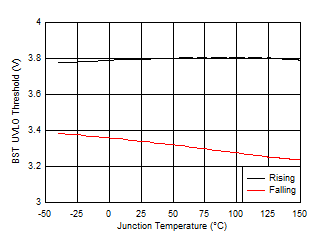
GUID-45F3FA1C-2F43-434A-AFC6-53A226AB11DC-low.gifFigure 7-13 BST UVLO Thresholds vs Junction Temperature
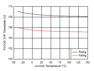
GUID-DAC0D346-B8BA-40E9-9778-5E729AEEB586-low.gifFigure 7-15 PGOOD OVP Thresholds vs Junction Temperature
GUID-531E6073-2786-40E6-A273-22E873F84B83-low.gif
 
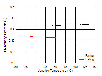
Figure 7-17 EN Standby Thresholds vs Junction Temperature
GUID-8B90119F-69B1-4AA7-B3C5-7AD4C756A2D1-low.gif
RRT = 25 kΩ
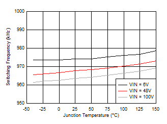
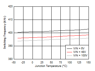
Figure 7-19 Oscillator Frequency vs Junction Temperature
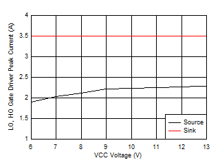
GUID-85261FEE-0BB2-492E-B2EE-4D4809545C8B-low.gifFigure 7-21 Gate Driver Peak Current vs VCC Voltage
GUID-629011A7-AF74-4EA8-887A-0C6CDCDAE740-low.gif
 
Figure 7-23 LO Driver Resistance vs VCC Voltage
GUID-55E5B1D9-0284-40C7-AC12-4CD93E2C747D-low.gif
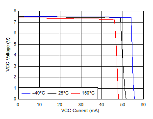
VIN = 5.5 V
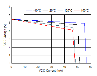
Figure 7-25 VCC vs ICC Characteristic
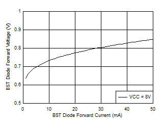
GUID-DB5D1971-B3CF-4D6D-ABF6-B1F97EB1C352-low.gifFigure 7-27 BST Diode Forward Voltage vs Current
GUID-93434958-1935-4FB1-8591-2F696879CBF3-low.gif
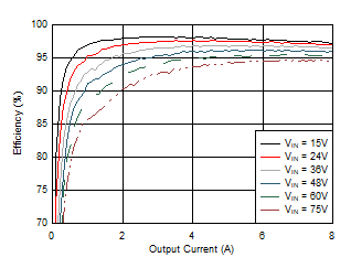
VOUT = 12 V FSW = 400 kHz
See Figure 9-16 RRT = 24.9 kΩ
Figure 7-2 Efficiency vs Load, CCM
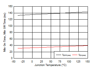
GUID-693E223B-28E0-4DCE-93BD-FD5FFC39C0B2-low.gifFigure 7-4 tON(min) and tOFF(min) vs Junction Temperature
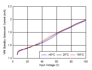
GUID-2F940003-37C5-4D6F-9196-3DB29F4A1063-low.gif
VSW = 0 V VEN/UVLO = 1 V
Figure 7-6 IQ-STANDBY vs Input Voltage
GUID-ABF27C0F-BAC4-4B4F-B16A-9EC4AFE51955-low.gif
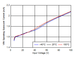
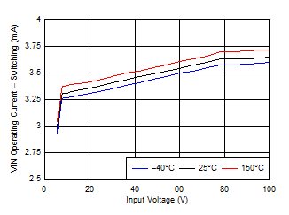
VSW = 0 V HO, LO Open
Figure 7-8 IQ-OPERATING (Switching) vs Input Voltage
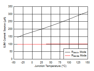
GUID-7528AA57-6D29-4ED8-B498-12A4AAB76FAA-low.gifFigure 7-10 ILIM Current Source vs Junction Temperature
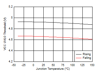
GUID-F158EAC2-667E-4283-A172-8A25DC5220AE-low.gifFigure 7-12 VCC UVLO Thresholds vs Junction Temperature
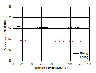
GUID-1337A5FC-267E-42CF-8C6D-024D62560EF1-low.gifFigure 7-14 PGOOD UVP Thresholds vs Junction Temperature
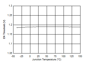
GUID-967691AA-A602-4EE4-8E85-47EF800EE44D-low.gifFigure 7-16 EN/UVLO Threshold vs Junction Temperature
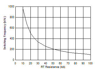
GUID-7681B1AA-5163-45F8-A491-FF895660D375-low.gif
VSW = 0 V
Figure 7-18 Oscillator Frequency vs RT Resistance
GUID-6008A2F6-6401-4B93-AFCD-D33985C746FE-low.gif
RRT = 10 kΩ
Figure 7-20 Oscillator Frequency vs Junction Temperature
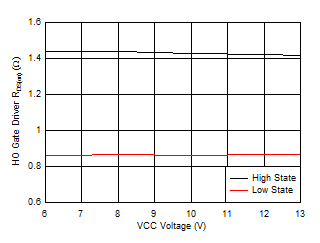
GUID-071DF25C-6023-4F8C-9FC3-6DC647D8A889-low.gifFigure 7-22 HO Driver Resistance vs VCC Voltage
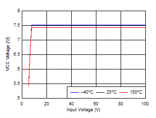
GUID-89639BFC-8270-479E-9631-F091F4519228-low.gif
VSS/TRK = 0 V
Figure 7-24 VCC Voltage vs Input Voltage
GUID-C531C91B-8012-456E-8D70-50EFB5CAC2E4-low.gif
VIN = 12 V
Figure 7-26 VCC vs ICC Characteristic
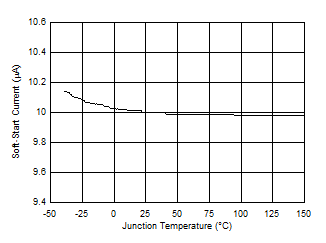
GUID-F611C726-94C8-471E-AAD7-30E030FDB4BF-low.gifFigure 7-28 SS/TRK Current Source vs Junction Temperature