SNVS300H July 2004 – September 2016 LM5111
PRODUCTION DATA.
- 1 Features
- 2 Applications
- 3 Description
- 4 Revision History
- 5 Device Options
- 6 Pin Configuration and Functions
- 7 Specifications
- 8 Detailed Description
- 9 Application and Implementation
- 10Power Supply Recommendations
- 11Layout
- 12Device and Documentation Support
- 13Mechanical, Packaging, and Orderable Information
封装选项
机械数据 (封装 | 引脚)
散热焊盘机械数据 (封装 | 引脚)
- DGN|8
订购信息
7 Specifications
7.1 Absolute Maximum Ratings
see (1)(2)| MIN | MAX | UNIT | |
|---|---|---|---|
| VCC to VEE | −0.3 | 15 | V |
| IN to VEE | −0.3 | 15 | V |
| Maximum junction temperature, TJ(max) | 150 | °C | |
| Storage temperature, Tstg | −55 | 150 | °C |
(1) Stresses beyond those listed under Absolute Maximum Ratings may cause permanent damage to the device. These are stress ratings only, which do not imply functional operation of the device at these or any other conditions beyond those indicated under Recommended Operating Conditions. Exposure to absolute-maximum-rated conditions for extended periods may affect device reliability.
(2) If Military/Aerospace specified devices are required, please contact the Texas Instruments Sales Office/Distributors for availability and specifications.
7.2 ESD Ratings
| VALUE | UNIT | |||
|---|---|---|---|---|
| V(ESD) | Electrostatic discharge | Human-body model (HBM), per ANSI/ESDA/JEDEC JS-001(1) | 2000 | V |
(1) JEDEC document JEP155 states that 500-V HBM allows safe manufacturing with a standard ESD control process.
7.3 Recommended Operating Conditions
over operating free-air temperature range (unless otherwise noted)| MIN | NOM | MAX | UNIT | ||
|---|---|---|---|---|---|
| TJ | Operating junction temperature | 125 | °C | ||
7.4 Thermal Information
| THERMAL METRIC(1) | LM5111 | UNIT | ||
|---|---|---|---|---|
| D (SOIC) |
DGN (MSOP-PowerPAD) |
|||
| 8 PINS | 8 PINS | |||
| RθJA | Junction-to-ambient thermal resistance | 112.2 | 50.7 | °C/W |
| RθJC(top) | Junction-to-case (top) thermal resistance | 54.6 | 56.6 | °C/W |
| RθJB | Junction-to-board thermal resistance | 53.1 | 35.9 | °C/W |
| ψJT | Junction-to-top characterization parameter | 9.4 | 5.3 | °C/W |
| ψJB | Junction-to-board characterization parameter | 52.5 | 35.6 | °C/W |
| RθJC(bot) | Junction-to-case (bottom) thermal resistance | N/A | 4.4 | °C/W |
(1) For more information about traditional and new thermal metrics, see the Semiconductor and IC Package Thermal Metrics application report.
7.5 Electrical Characteristics
TJ = −40°C to +125°C, VCC = 12 V, VEE = 0 V, No Load on OUT_A or OUT_B, unless otherwise specified.| PARAMETER | TEST CONDITIONS | MIN | TYP | MAX | UNIT | |
|---|---|---|---|---|---|---|
| VCC operating range | VCC−VEE | 3.5 | 14 | V | ||
| VCCR | VCC undervoltage lockout (rising) | VCC−VEE | 2.3 | 2.9 | 3.5 | V |
| VCCH | VCC undervoltage lockout hysteresis | 230 | mV | |||
| ICC | VCC supply current (ICC) | IN_A = IN_B = 0 V (5111-1) | 1 | 2 | mA | |
| IN_A = IN_B = VCC (5111-2) | 1 | 2 | ||||
| IN_A = VCC, IN_B = 0 V (5111-3) | 1 | 2 | ||||
| CONTROL INPUTS | ||||||
| VIH | Logic high | 2.2 | V | |||
| VIL | Logic low | 0.8 | V | |||
| VthH | High threshold | 1.3 | 1.75 | 2.2 | V | |
| VthL | Low threshold | 0.8 | 1.35 | 2 | V | |
| HYS | Input hysteresis | 400 | mV | |||
| IIL | Input current low | IN_A=IN_B=VCC (5111-1-2-3) | –1 | 0.1 | 1 | µA |
| IIH | Input current high | IN_B=VCC (5111-3) | 10 | 18 | 25 | |
| IN_A=IN_B=VCC (5111-2) | –1 | 0.1 | 1 | |||
| IN_A=IN_B=VCC (5111-1) | 10 | 18 | 25 | |||
| IN_A=VCC (5111-3) | –1 | 0.1 | 1 | |||
| OUTPUT DRIVERS | ||||||
| ROH | Output resistance high | IOUT = −10 mA(1) | 30 | 50 | Ω | |
| ROL | Output resistance low | IOUT = + 10 mA(1) | 1.4 | 2.5 | Ω | |
| ISource | Peak source current | OUTA/OUTB = VCC/2, 200-ns Pulsed Current |
3 | A | ||
| ISink | Peak sink current | OUTA/OUTB = VCC/2, 200-ns Pulsed Current |
5 | A | ||
| LATCHUP PROTECTION | ||||||
| AEC - Q100, method 004 | TJ = 150°C | 500 | mA | |||
| THERMAL RESISTANCE | ||||||
| θJA | Junction to ambient, 0 LFPM air flow |
SOIC Package | 170 | °C/W | ||
| MSOP-PowerPAD Package | 60 | |||||
| θJC | Junction to case | SOIC Package | 70 | °C/W | ||
| MSOP-PowerPAD Package | 4.7 | |||||
(1) The output resistance specification applies to the MOS device only. The total output current capability is the sum of the MOS and Bipolar devices.
7.6 Switching Characteristics
over operating free-air temperature range (unless otherwise noted)| PARAMETER | TEST CONDITIONS | MIN | TYP | MAX | UNIT | |
|---|---|---|---|---|---|---|
| td1 | Propagation delay time low to high, IN rising (IN to OUT) | CLOAD = 2 nF(1) | 25 | 40 | ns | |
| td2 | Propagation delay time high to low, IN falling (IN to OUT) | CLOAD = 2 nF(1) | 25 | 40 | ns | |
| tr | Rise time | CLOAD = 2 nF(1) | 14 | 25 | ns | |
| tf | Fall time | CLOAD = 2 nF(1) | 12 | 25 | ns | |
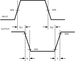 Figure 1. Inverting
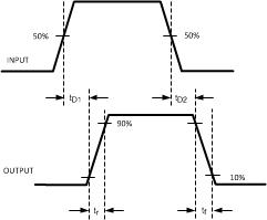 Figure 2. Noninverting
7.7 Typical Characteristics
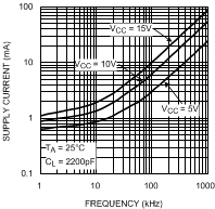 Figure 3. Supply Current vs Frequency
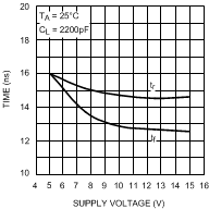 Figure 5. Rise and Fall Time vs Supply Voltage
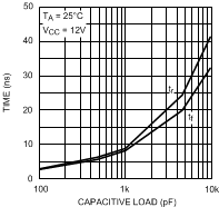 Figure 7. Rise and Fall Time vs Capacitive Load
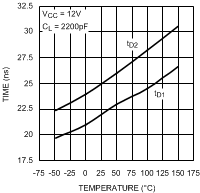 Figure 9. Delay Time vs Temperature
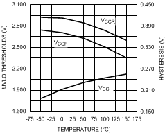 Figure 11. UVLO Thresholds and Hysteresis vs Temperature
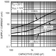 Figure 4. Supply Current vs Capacitive Load
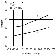 Figure 6. Rise and Fall Time vs Temperature
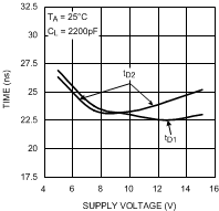 Figure 8. Delay Time vs Supply Voltage
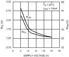 Figure 10. RDSON vs Supply Voltage