SNVS631D January   2010  – October 2016 LM5035C

PRODUCTION DATA.  

  1. Features
  2. Applications
  3. Description
  4. Revision History
  5. Device Comparison Table
  6. Pin Configuration and Functions
  7. Specifications
    1. 7.1 Absolute Maximum Ratings
    2. 7.2 ESD Ratings
    3. 7.3 Recommended Operating Conditions
    4. 7.4 Thermal Information
    5. 7.5 Electrical Characteristics
    6. 7.6 Typical Characteristics
  8. Detailed Description
    1. 8.1 Overview
    2. 8.2 Functional Block Diagram
    3. 8.3 Feature Description
      1. 8.3.1  High-Voltage Start-Up Regulator
      2. 8.3.2  Line Undervoltage Detector
      3. 8.3.3  Line Overvoltage, Load Overvoltage, and Remote Thermal Protection
      4. 8.3.4  Reference
      5. 8.3.5  Cycle-by-Cycle Current Limit
      6. 8.3.6  Overload Protection Timer
      7. 8.3.7  Soft Start
      8. 8.3.8  PWM Comparator
      9. 8.3.9  Feedforward Ramp and Volt • Second Clamp
      10. 8.3.10 Oscillator, Sync Capability
      11. 8.3.11 Gate Driver Outputs (HO and LO)
      12. 8.3.12 Synchronous Rectifier Control Outputs (SR1 and SR2)
      13. 8.3.13 Thermal Protection
    4. 8.4 Device Functional Modes
  9. Application and Implementation
    1. 9.1 Application Information
    2. 9.2 Typical Application
      1. 9.2.1 Design Requirements
      2. 9.2.2 Detailed Design Procedure
        1. 9.2.2.1 VIN
        2. 9.2.2.2 For Applications >100 V
        3. 9.2.2.3 Current Sense
        4. 9.2.2.4 HO, HB, HS, and LO
        5. 9.2.2.5 Programmable Delay (DLY)
        6. 9.2.2.6 UVLO and OVP Voltage Divider Selection For R1, R2, and R3
        7. 9.2.2.7 Fault Protection
        8. 9.2.2.8 Hiccup Mode Current Limit Restart (RES)
      3. 9.2.3 Application Curves
  10. 10Power Supply Recommendations
  11. 11Layout
    1. 11.1 Layout Guidelines
    2. 11.2 Layout Example
  12. 12Device and Documentation Support
    1. 12.1 Documentation Support
      1. 12.1.1 Related Documentation
    2. 12.2 Receiving Notification of Documentation Updates
    3. 12.3 Community Resource
    4. 12.4 Trademarks
    5. 12.5 Electrostatic Discharge Caution
    6. 12.6 Glossary
  13. 13Mechanical, Packaging, and Orderable Information

封装选项

机械数据 (封装 | 引脚)
散热焊盘机械数据 (封装 | 引脚)
订购信息

Specifications

Absolute Maximum Ratings

over operating free-air temperature range (unless otherwise noted)(1)(2)
MIN MAX UNIT
VIN to GND –0.3 105 V
HS to GND –1 105 V
HB to GND –0.3 118 V
HB to HS –0.3 18 V
VCC to GND –0.3 16 V
RT, DLY to GND –0.3 5.5 V
COMP input current 10 mA
CS 1 V
All other inputs to GND –0.3 7 V
Junction temperature 150 °C
Storage temperature –65 150 °C
Stresses beyond those listed under Absolute Maximum Ratings may cause permanent damage to the device. These are stress ratings only, which do not imply functional operation of the device at these or any other conditions beyond those indicated under Recommended Operating Conditions. Exposure to absolute-maximum-rated conditions for extended periods may affect device reliability.
If Military/Aerospace specified devices are required, contact the Texas Instruments Sales Office/ Distributors for availability and specifications.

ESD Ratings

VALUE UNIT
V(ESD) Electrostatic discharge Human-body model (HBM), per ANSI/ESDA/JEDEC JS-001(1) ±1500 V
Charged-device model (CDM), per JEDEC specification JESD22-C101(2) ±250
JEDEC document JEP155 states that 500-V HBM allows safe manufacturing with a standard ESD control process.
JEDEC document JEP157 states that 250-V CDM allows safe manufacturing with a standard ESD control process.

Recommended Operating Conditions

over operating free-air temperature range (unless otherwise noted)(1)
MIN NOM MAX UNIT
VIN voltage 13 105 V
External voltage applied to VCC 8 15 V
Operating junction temperature –40 125 °C
Absolute Maximum Ratings are limits beyond which damage to the device may occur. Operating Ratings are conditions under which operation of the device is intended to be functional. For ensured specifications and test conditions, see Electrical Characteristics.

Thermal Information

THERMAL METRIC(1) LM5035C UNIT
PWP (HTSSOP) NHZ (WQFN)
20 PINS 24 PINS
RθJA Junction-to-ambient thermal resistance 35.9 31.3 °C/W
RθJC(top) Junction-to-case (top) thermal resistance 19.8 25 °C/W
RθJB Junction-to-board thermal resistance 16.7 9.9 °C/W
ψJT Junction-to-top characterization parameter 0.4 0.2 °C/W
ψJB Junction-to-board characterization parameter 16.6 10.1 °C/W
RθJC(bot) Junction-to-case (bottom) thermal resistance 1.6 1.6 °C/W
For more information about traditional and new thermal metrics, see the Semiconductor and IC Package Thermal Metrics application report.

Electrical Characteristics

Specifications with standard typeface are for TJ = 25°C, unless indicating that type applies over full operating junction temperature range. VVIN = 48 V, VVCC = 10 V externally applied, RRT = 15 kΩ, RDLY = 27.4 kΩ, VUVLO = 3 V, VOVP = 0 V unless otherwise stated. See (1) and (2).
PARAMETER TEST CONDITIONS MIN TYP MAX UNIT
START-UP REGULATOR (VCC PIN)
VVCC VCC voltage IVCC = 10 mA TJ = 25°C 7.6 V
TJ = –40°C to 125°C 7.3 7.9
IVCC(LIM) VCC current limit VVCC = 7 V, TJ = –40°C to 125°C 58 mA
VVCCUV VCC undervoltage threshold (VCC increasing) VIN = VCC, ΔVVCC from the regulation setpoint TJ = 25°C 0.1 V
TJ = –40°C to 125°C 0.2
VCC decreasing VCC – PGND TJ = 25°C 6.2 V
TJ = –40°C to 125°C 5.5 6.9
IVIN Start-up regulator current VIN = 90 V, UVLO = 0 V TJ = 25°C 30 µA
TJ = –40°C to 125°C 70
Supply current into VCC from external source Outputs and COMP open,
VVCC = 10 V, Outputs Switching
TJ = 25°C 4 mA
TJ = –40°C to 125°C 6
VOLTAGE REFERENCE REGULATOR (REF PIN)
VREF REF voltage IREF = 0 mA TJ = 25°C 5 V
TJ = –40°C to 125°C 4.85 5.15
REF voltage regulation IREF = 0 to 10 mA TJ = 25°C 25 mV
TJ = –40°C to 125°C 50
REF current limit REF = 4.5 V TJ = 25°C 20 mA
TJ = –40°C to 125°C 15
UNDERVOLTAGE LOCKOUT AND SHUTDOWN (UVLO PIN)
VUVLO Undervoltage threshold TJ = 25°C 1.25 V
TJ = –40°C to 125°C 1.212 1.288
IUVLO Hysteresis current UVLO pin sinking TJ = 25°C 23 µA
TJ = –40°C to 125°C 19 27
Undervoltage shutdown threshold UVLO voltage falling 0.3 V
Undervoltage standby enable threshold UVLO voltage rising 0.4 V
OVERVOLTAGE PROTECTION (OVP PIN)
VOVP Overvoltage threshold TJ = 25°C 1.25 V
TJ = –40°C to 125°C 1.212 1.288
IOVP Hysteresis current OVP pin sourcing TJ = 25°C 23 µA
TJ = –40°C to 125°C 19 27
CURRENT SENSE INPUT (CS PIN)
VCS Current limit threshold TJ = 25°C 0.25 V
TJ = –40°C to 125°C 0.288 0.272
CS delay to output CS from zero to 1 V. Time for HO and LO to fall to 90% of VCC. Output load = 0 pF. 80 ns
Leading edge blanking time at CS 50 ns
CS sink impedance (clocked) Internal FET sink impedance TJ = 25°C 32 Ω
TJ = –40°C to 125°C 60
CURRENT LIMIT RESTART (RES PIN)
VRES RES threshold TJ = 25°C 2.5 V
TJ = –40°C to 125°C 2.4 2.6
Charge source current VRES = 1.5 V TJ = 25°C 22 µA
TJ = –40°C to 125°C 16 28
Discharge sink current VRES = 1 V TJ = 25°C 12 µA
TJ = –40°C to 125°C 8 16
SOFT-START (SS PIN)
ISS Charging current in normal operation VSS = 0 TJ = 25°C 110 µA
TJ = –40°C to 125°C 80 140
Charging current during a hiccup mode restart VSS = 0 TJ = 25°C 1.2 µA
TJ = –40°C to 125°C 0.6 1.8
OSCILLATOR (RT PIN)
FSW1 Frequency 1 (at HO, half oscillator frequency) RRT = 15 kΩ TJ = 25°C 200 kHz
TJ = –40°C to 125°C 185 215
RRT = 15 kΩ TJ = –40°C to 125°C 180 220
FSW2 Frequency 2 (at HO, half oscillator frequency) RRT = 5.49 kΩ TJ = 25°C 500 kHz
TJ = –40°C to 125°C 430 570
DC level 2 V
Input sync threshold TJ = 25°C 3 V
TJ = –40°C to 125°C 2.5 3.4
PWM CONTROLLER (COMP PIN)
Delay to output 80 ns
VPWM-OS SS to RAMP offset TJ = 25°C 1 V
TJ = –40°C to 125°C 0.7 1.2
Minimum duty cycle SS = 0 V TJ = –40°C to 125°C 0%
Small signal impedance ICOMP = 600 µA, COMP current to PWM voltage 6200 Ω
MAIN OUTPUT DRIVERS (HO AND LO PINS)
Output high voltage IOUT = 50 mA, VHB - VHO, VVCC - VLO TJ = 25°C 0.25 V
TJ = –40°C to 125°C 0.5
Output low voltage IOUT = 100 mA TJ = 25°C 0.2 V
TJ = –40°C to 125°C 0.5
Rise time CLOAD = 1 nF 15 ns
Fall time CLOAD = 1 nF 13 ns
Peak source current VHO,LO = 0 V, VVCC = 10 V 1.25 A
Peak sink current VHO,LO = 10 V, VVCC = 10 V 2 A
HB threshold VCC rising 3.8 V
VOLTAGE FEED-FORWARD (RAMP PIN)
RAMP comparator threshold COMP current = 0 TJ = 25°C 2.5 V
TJ = –40°C to 125°C 2.4 2.6
SYNCHRONOUS RECTIFIER DRIVERS (SR1, SR2)
Output high voltage IOUT = 5 mA, VREF - VSR1, VREF - VSR2 TJ = 25°C 0.1 V
TJ = –40°C to 125°C 0.25
Output low voltage IOUT = 10 mA (sink) TJ = 25°C 0.08 V
TJ = –40°C to 125°C 0.2
Rise time CLOAD = 1 nF 40 ns
Fall time CLOAD = 1 nF 20 ns
Peak source current VSR = 0 0.09 A
Peak sink current VSR = VREF 0.2 A
T1 Dead time, SR1 falling to HO rising, SR2 falling to LO rising RDLY = 10 k 33 ns
RDLY = 27.4 k TJ = 25°C 86 ns
TJ = –40°C to 125°C 68 120
RDLY = 100 k 300 ns
T2 Dead time, HO falling to SR1 rising, LO falling to SR2 rising RDLY = 10 k 18 ns
RDLY = 27.4 k TJ = 25°C 26 ns
TJ = –40°C to 125°C 15 39
RDLY = 100 k 80 ns
THERMAL SHUTDOWN
TSD Shutdown temperature 165 °C
Hysteresis 20 °C
All limits are ensured. All electrical characteristics having room temperature limits are tested during production with TA = 25°C. All hot and cold limits are ensured by correlating the electrical characteristics to process and temperature variations and applying statistical process control.
Typical specifications represent the most likely parametric norm at 25°C operation

Typical Characteristics

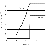
LM5035C 30106805.gif
Figure 1. VVCC and VREF vs VVIN
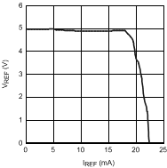
LM5035C 30106807.gif
Figure 3. VREF vs IREF
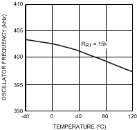
LM5035C 30106809.gif
Figure 5. Oscillator Frequency vs Temperature
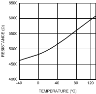
LM5035C 30106811.gif
Figure 7. Effective Comp Input Impedance
LM5035C 30106813.gif
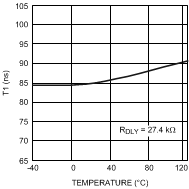
Figure 9. SR T1 Parameter vs Temperature
LM5035C 30106806.gif
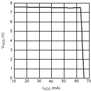
Figure 2. VVCC vs IVCC
LM5035C 30106808.gif
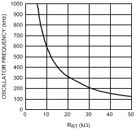
Figure 4. Frequency vs RT
LM5035C 30106810.gif
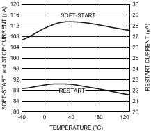
Figure 6. Soft-Start Current vs Temperature
LM5035C 30106812.gif
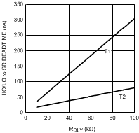
Figure 8. RDLY vs Dead Time
LM5035C 30106814.gif
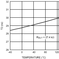
Figure 10. SR T2 Parameter vs Temperature