SNVS344B March 2005 – December 2014 LM5032
PRODUCTION DATA.
- 1 Features
- 2 Applications
- 3 Description
- 4 Revision History
- 5 Pin Configuration and Functions
- 6 Specifications
-
7 Detailed Description
- 7.1 Overview
- 7.2 Functional Block Diagram
- 7.3
Feature Description
- 7.3.1 Line Undervoltage Lock Out, UVLO, Shutdown
- 7.3.2 Startup Regulator, VIN, VCC
- 7.3.3 Drivers Off, VCC Disable
- 7.3.4 Oscillator
- 7.3.5 PWM Comparator/Slope Compensation
- 7.3.6 Cycle-by-Cycle Current Limit
- 7.3.7 Hiccup Mode Current Limit Restart
- 7.3.8 Soft-Start
- 7.3.9 Output Duty Cycle
- 7.3.10 Driver Outputs
- 7.3.11 Thermal Shutdown
- 7.4 Device Functional Modes
-
8 Application and Implementation
- 8.1 Application Information
- 8.2 Typical Application
- 9 Power Supply Recommendations
- 10Layout
- 11Device and Documentation Support
- 12Mechanical, Packaging, and Orderable Information
5 Pin Configuration and Functions
PW Package
16-Pin TSSOP
Top View
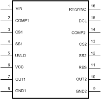
Pin Functions
| PIN | I/O | DESCRIPTION | APPLICATIONS INFORMATION | |
|---|---|---|---|---|
| NO. | NAME | |||
| 1 | VIN | P | Input Supply | Input to the startup regulator. The operating input range is 13 V to 100 V with transient capability to 105 V. |
| 2 | COMP1 | I | PWM Control, Controller 1 | The COMP1 input provides voltage feedback to the PWM comparator inverting input of Controller 1 through a 3:1 divider. The OUT1 duty cycle increases as the COMP1 voltage increases. An internal 5-KΩ pull-up resistor to 5.0-V provides bias current to an opto-coupler transistor. |
| 3 | CS1 | I | Current Sense Input, Controller 1 | Input for current mode control and the current limit sensing. If the CS1 pin exceeds 0.5V the OUT1 pulse is terminated producing cycle-by-cycle current limiting. External resistance connected to CS1 will adjust (increase) PWM slope compensation. This pin's voltage must not exceed 1.25V. |
| 4 | SS1 | I | Soft-start, Controller 1 | An internal 50-µA current source charges an external capacitor to set the soft-start rate. During a current limit restart sequence, the internal current source is reduced to 1 µA to increase the delay before retry. Forcing SS1 below 0.5 V shuts off Controller 1. |
| 5 | UVLO | I | VIN Under-Voltage Lockout | An external resistor divider sets the input voltage threshold to enable the LM5032. The UVLO comparator reference voltage is 1.25 V. A switched 20-µA current source provides adjustable UVLO hysteresis. The UVLO pin voltage also controls the maximum duty cycle as described in the Feature Description section. |
| 6 | VCC | P | Start-up regulator output | Output of the 7.7-V high-voltage start-up regulator. Current limit is a minimum of 19 mA. |
| 7 | OUT1 | O | Main Gate Driver, Controller 1 | Gate driver output to the primary side switch for Controller 1. OUT1 swings between VCC and GND1 at a frequency equal to half the oscillator frequency. |
| 8 | GND1 | G | Ground, Controller 1 | Ground connection for Controller 1 including gate driver, PWM controller, soft-start and support functions. |
| 9 | GND2 | G | Ground, Controller 2 | Ground connection for Controller 2 including the gate driver, PWM controller and soft-start. |
| 10 | OUT2 | O | Main Gate Driver, Controller 2 | Gate driver output to the primary side switch for Controller 2. OUT2 swings between VCC and GND2 at a frequency equal to half the oscillator frequency. |
| 11 | RES | I | Hiccup mode restart adjust | An external capacitor sets the time delay before forced restart during a sustained period of cycle-by-cycle current limiting. The hiccup mode comparator threshold is 2.55 V. |
| 12 | SS2 | I | Soft-start, Controller 2 | An internal 50-µA current source charges an external capacitor to set the soft-start rate. During a current limit restart sequence, the internal current source is reduced to 1 µA to increase the delay before retry. Forcing SS2 below 0.5 V shuts off Controller 2. |
| 13 | CS2 | I | Current Sense Input, Controller 2 | Input for current mode control and the current limit sensing. If the CS2 pin exceeds 0.5 V the OUT2 pulse is terminated producing cycle-by-cycle current limiting. External resistance connected to CS2 will adjust (increase) PWM slope compensation. This pin's voltage must not exceed 1.25V. |
| 14 | COMP2 | I | PWM Control, Controller 2 | The COMP2 input provides voltage feedback to the PWM comparator inverting input of Controller 2 through a 3:1 divider. The OUT2 duty cycle increases as the COMP2 voltage increases. An internal 5kΩ pull-up resistor to 5.0 V provides bias current to the opto-coupler transistor. |
| 15 | DCL | I | Duty Cycle Limit | An external resistor sets the maximum allowed duty cycle at OUT1 and OUT2. |
| 16 | RT/SYNC | I | Oscillator Adjust and Synchronizing input | An external resistor sets the oscillator frequency. This pin also accepts ac-coupled synchronization pulses from an external source. |