SNVS344B March 2005 – December 2014 LM5032
PRODUCTION DATA.
- 1 Features
- 2 Applications
- 3 Description
- 4 Revision History
- 5 Pin Configuration and Functions
- 6 Specifications
-
7 Detailed Description
- 7.1 Overview
- 7.2 Functional Block Diagram
- 7.3
Feature Description
- 7.3.1 Line Undervoltage Lock Out, UVLO, Shutdown
- 7.3.2 Startup Regulator, VIN, VCC
- 7.3.3 Drivers Off, VCC Disable
- 7.3.4 Oscillator
- 7.3.5 PWM Comparator/Slope Compensation
- 7.3.6 Cycle-by-Cycle Current Limit
- 7.3.7 Hiccup Mode Current Limit Restart
- 7.3.8 Soft-Start
- 7.3.9 Output Duty Cycle
- 7.3.10 Driver Outputs
- 7.3.11 Thermal Shutdown
- 7.4 Device Functional Modes
-
8 Application and Implementation
- 8.1 Application Information
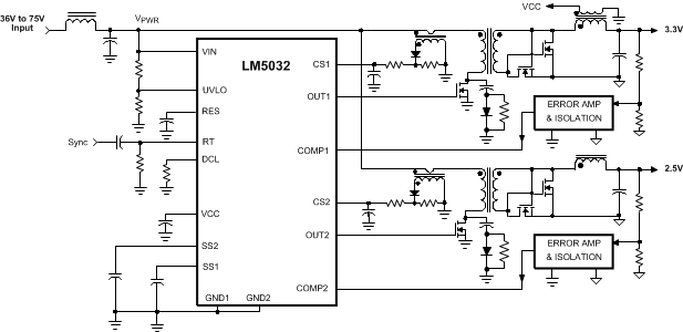
- 8.2 Typical Application
- 9 Power Supply Recommendations
- 10Layout
- 11Device and Documentation Support
- 12Mechanical, Packaging, and Orderable Information
1 Features
- Two Independent PWM Current Mode Controllers
- Integrated High-Voltage Startup Regulator
- Compound 2.5-A Main Output Gate Drivers
- Single Resistor Oscillator Setting to 2 MHz
- Synchronizable Oscillator
- Programmable Maximum Duty Cycle
- Maximum Duty Cycle Fold-Back at High-Line Voltage
- Adjustable Timer for Hiccup Mode Current Limiting
- Integrated Slope Compensation
- Adjustable Line Undervoltage Lockout
- Independently Adjustable Soft-Start (Each Regulator)
- Direct Interface with Opto-Coupler Transistor
- Thermal Shutdown
- TSSOP 16-Pin Package
2 Applications
- Telecommunication Power Converters
- Industrial Power Converters
- 42-V Automotive Systems
3 Description
The LM5032 dual current mode PWM controller contains all the features needed to control either two independent forward dc/dc converters or a single high current converter comprised of two interleaved power stages. The two controller channels operate 180° out of phase thereby reducing input ripple current. The LM5032 includes a startup regulator that operates over a wide input range up to 100 V and compound (bipolar + CMOS) gate drivers that provide a robust 2.5-A peak sink current. The adjustable maximum PWM duty cycle reduce stress on the primary side MOSFET switches. Additional features include programmable line undervoltage lockout, cycle-by-cycle current limit, hiccup mode fault operation with adjustable response time, PWM slope compensation, soft-start, and a 2-MHz capable oscillator with synchronization capability.
Device Information(1)
| PART NUMBER | PACKAGE | BODY SIZE (NOM) |
|---|---|---|
| LM5032 | TSSOP (16) | 5.00 mm x 4.40 mm |
- For all available packages, see the orderable addendum at the end of the datasheet.
Typical Application Circuit