SNVS363E August 2005 – November 2015 LM5026
PRODUCTION DATA.
- 1 Features
- 2 Applications
- 3 Description
- 4 Revision History
- 5 Pin Configuration and Functions
- 6 Specifications
-
7 Detailed Description
- 7.1 Overview
- 7.2 Functional Block Diagram
- 7.3
Feature Description
- 7.3.1 High Voltage Start-Up Regulator
- 7.3.2 Line Undervoltage Detector
- 7.3.3 PWM Outputs
- 7.3.4 Gate Driver Outputs
- 7.3.5 PWM Comparator/Slope Compensation
- 7.3.6 Maximum Duty Cycle Clamp
- 7.3.7 Soft-Start / Soft-Stop
- 7.3.8 Current Sense and Current Limit
- 7.3.9 Overload Protection Timer
- 7.3.10 Oscillator and Sync Capability
- 7.3.11 Thermal Protection
- 7.4 Device Functional Modes
-
8 Application and Implementation
- 8.1 Application Information
- 8.2 Typical Application
- 9 Power Supply Recommendations
- 10Layout
- 11Device and Documentation Support
- 12Mechanical, Packaging, and Orderable Information
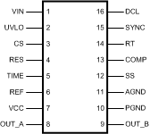
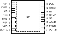
5 Pin Configuration and Functions
PW Package
16-Pin TSSOP
Top View

NHQ Package
16-Pin WSON
Top View

Pin Functions
| PIN | TYPE(1) | DESCRIPTION | |
|---|---|---|---|
| NO. | NAME | ||
| 1 | VIN | I | Input voltage source. Input to the start-up regulator. Operating input range is 13 V to 100 V with transient capability to 105 V. For power sources outside of this range, the LM5026 can be biased directly at VCC by an external regulator. |
| 2 | UVLO | I | Line undervoltage lockout. An external voltage divider from the power source sets the shutdown and standby comparator levels. When UVLO reaches the 0.4-V threshold the VCC and REF regulators are enabled. At the 1.25-V threshold the SS pin is released and the device enters the active mode. |
| 3 | CS | I | Current Sense input for current mode control and current limit. If CS exceeds 0.5 V, the output pulse will be terminated, entering cycle-by-cycle current limit. An internal switch holds CS low for 100 nS after OUT_A switches high to blank leading edge transients. |
| 4 | RES | I | Restart Timer. If cycle-by-cycle current limit is reached during any cycle, a 10-µA current is sourced to the RES pin capacitor. If the RES capacitor voltage reaches 2.5 V, the soft-start capacitor will be fully discharged and then released with a pullup current of 1 µA. After the first output pulse at OUT_A (when SS = 1.4 V), the SS pin charging current will revert back to 50 µA. |
| 5 | TIME | I | Gate drive overlap or deadtime control. An external resistor (RSET) sets either the overlap time or deadtime for the active clamp output. An RSET resistor connected between TIME and AGND produces in-phase OUT_A and OUT_B pulses with overlap. An RSET resistor connected between TIME and REF produces out-of-phase OUT_A and OUT_B pulses with deadtime. |
| 6 | REF | O | Output of 5-V reference. Maximum output current is 10 mA. Locally decouple with a 0.1-µF capacitor. |
| 7 | VCC | P | Output of the high voltage start-up regulator. The VCC voltage is regulated to 7.6 V. If an auxiliary winding raises the voltage on this pin above the regulation setpoint, the internal start-up regulator will shutdown, thus reducing the IC power dissipation. |
| 8 | OUT_A | O | Main output driver. Output of the main switch PWM gate driver. Capable of 3-A peak sink current. |
| 9 | OUT_B | O | Active clamp output driver. Output of the active clamp switch gate driver. Capable of 0.5-A peak source and sink current. |
| 10 | PGND | G | Power ground. Connect directly to analog cround. |
| 11 | AGND | G | Analog return. Connect directly to power cround. |
| 12 | SS | I | Soft-start. An external capacitor and an internal 50-µA current source set the soft-start ramp. The SS current source is reduced to 1 µA following a restart event. The soft-stop discharge current is 50 µA. |
| 13 | COMP | I | Input to the pulse width modulator. The external optocoupler connected to the COMP pin sources current into an internal NPN current mirror. The PWM duty cycle is maximum with zero input current, while 1 mA reduces the duty cycle to zero. The current mirror improves the frequency response by reducing the ac voltage across the optocoupler detector. |
| 14 | RT | I | Oscillator frequency control. Normally biased at 2 V. The total external resistance connected between RT and AGND sets the internal oscillator frequency. |
| 15 | SYNC | I/O | Oscillator synchronization input/output. The internal oscillator can be synchronized to an external clock with an external pulldown device. Multiple LM5026 devices can be synchronized together by connection of their SYNC pins. |
| 16 | DCL | I | Maximum duty cycle control. An external resistor divider connected from RT to AGND sets the maximum output duty cycle for OUT_A. |
| EP | Exposed Pad (WSON Package Only) | G | Exposed Pad, underside of WSON package. Connect to system ground plane for reduced thermal resistance. |
(1) P = Power, G = Ground, I = Input, O = Output, I/O = Input/Output