SNVS608H June 2009 – September 2016 LM5009A
PRODUCTION DATA.
- 1 Features
- 2 Applications
- 3 Description
- 4 Revision History
- 5 Pin Configuration and Functions
- 6 Specifications
- 7 Detailed Description
- 8 Application and Implementation
- 9 Power Supply Recommendations
- 10Layout
- 11Device and Documentation Support
- 12Mechanical, Packaging, and Orderable Information
6 Specifications
6.1 Absolute Maximum Ratings
over operating free-air temperature range (unless otherwise noted)(1)| MIN | MAX | UNIT | ||
|---|---|---|---|---|
| VIN to GND | –0.3 | 100 | V | |
| BST to GND | –0.3 | 114 | V | |
| SW to GND (steady state) | –1 | V | ||
| BST to VCC | 100 | V | ||
| BST to SW | 14 | V | ||
| VCC to GND | 14 | V | ||
| All other inputs to GND | –0.3 | 7 | V | |
| Storage temperature, Tstg | –55 | 150 | °C | |
(1) Stresses beyond those listed under Absolute Maximum Ratings may cause permanent damage to the device. These are stress ratings only, which do not imply functional operation of the device at these or any other conditions beyond those indicated under Recommended Operating Conditions. Exposure to absolute-maximum-rated conditions for extended periods may affect device reliability.
6.2 ESD Ratings
| VALUE | UNIT | |||
|---|---|---|---|---|
| V(ESD) | Electrostatic discharge | Human-body model (HBM), per ANSI/ESDA/JEDEC JS-001(1) | ±2000 | V |
| Charged-device model (CDM), per JEDEC specification JESD22-C101(2) | ±750 | |||
(1) JEDEC document JEP155 states that 500-V HBM allows safe manufacturing with a standard ESD control process.
(2) JEDEC document JEP157 states that 250-V CDM allows safe manufacturing with a standard ESD control process.
6.3 Recommended Operating Conditions
over operating free-air temperature range (unless otherwise noted)| MIN | MAX | UNIT | ||
|---|---|---|---|---|
| VIN | Input voltage | 6 | 95 | V |
| TJ | Operating junction temperature | –40 | 125 | °C |
6.4 Thermal Information
| THERMAL METRIC(1) | LM5009A | UNIT | ||
|---|---|---|---|---|
| DGK (VSSOP) | NGU (WSON) | |||
| 8 PINS | 8 PINS | |||
| RθJA | Junction-to-ambient thermal resistance | 157.7 | 42.8 | °C/W |
| RθJC(top) | Junction-to-case (top) thermal resistance | 50.2 | 41.5 | °C/W |
| RθJB | Junction-to-board thermal resistance | 77.9 | 20.1 | °C/W |
| ψJT | Junction-to-top characterization parameter | 4.5 | 0.4 | °C/W |
| ψJB | Junction-to-board characterization parameter | 76.5 | 20.2 | °C/W |
| RθJC(bot) | Junction-to-case (bottom) thermal resistance | — | 4.5 | °C/W |
(1) For more information about traditional and new thermal metrics, see the Semiconductor and IC Package Thermal Metrics application report.
6.5 Electrical Characteristics
Typical values correspond to TJ = 25 ° C. Minimum and maximum limits apply over TJ = –40°C to 125°C for LM5009A. Unless otherwise stated, VIN = 48 V(1)| PARAMETER | TEST CONDITIONS | MIN | TYP | MAX | UNIT | ||
|---|---|---|---|---|---|---|---|
| VCC SUPPLY | |||||||
| VCC Reg | VCC regulator output(2) | VIN = 48 V | 6.6 | 7 | 7.4 | V | |
| VIN – VCC | 6 V < VIN < 8.5 V | 100 | mV | ||||
| VCC bypass threshold | VIN increasing | 8.5 | V | ||||
| VCC bypass hysteresis | 300 | mV | |||||
| VCC output impedance | VIN = 6 V | 100 | Ω | ||||
| VIN = 10 V | 8.8 | Ω | |||||
| VIN = 48 V | 0.8 | Ω | |||||
| VCC current limit | VIN = 48 V | 9.2 | mA | ||||
| VCC UVLO | VCC increasing | 5.3 | V | ||||
| VCC UVLO hysteresis | 190 | mV | |||||
| VCC UVLO filter delay | 3 | µs | |||||
| Iin operating current | FB = 3 V, VIN = 48 V | 550 | 750 | µA | |||
| Iin shutdown current | RT/SD = 0 V | 110 | 176 | µA | |||
| CURRENT LIMIT | |||||||
| Current limit threshold | 0.24 | 0.3 | 0.36 | A | |||
| Current limit response time | Iswitch overdrive = 0.1 A, time to switch off | 350 | ns | ||||
| TOFF-1 | OFF-time generator | FB = 0 V, RCL = 100 K | 35 | µs | |||
| TOFF-2 | OFF-time generator | FB = 2.3 V, RCL = 100 K | 2.56 | µs | |||
| ON TIME GENERATOR | |||||||
| TON-1 | ON-time generator | VIN = 10 V, RON = 200 K | 2.15 | 2.77 | 3.5 | µs | |
| TON-2 | ON-time generator | VIN = 95 V, RON = 200 K | 200 | 300 | 420 | ns | |
| RT/SD | Remote shutdown threshold | Rising | 0.4 | 0.7 | 1.05 | V | |
| RT/SD(HYS) | Remote shutdown hysteresis | 35 | mV | ||||
| MINIMUM OFF TIME | |||||||
| Minimum off timer | FB = 0 V | 300 | ns | ||||
| REGULATION AND OV COMPARATORS | |||||||
| FB reference threshold | Internal reference, trip point for switch ON | 2.445 | 2.5 | 2.55 | V | ||
| FB overvoltage threshold | Trip point for switch OFF | 2.875 | V | ||||
| FB bias current | 100 | nA | |||||
| THERMAL SHUTDOWN | |||||||
| TSD | Thermal shutdown temperature | 165 | °C | ||||
| Thermal shutdown hysteresis | 25 | °C | |||||
(1) All minimum and maximum limits are specified by correlating the electrical characteristics to process and temperature variations and applying statistical process control. The junction temperature (TJ in °C) is calculated from the ambient temperature (TA in °C) and power dissipation (PD in Watts) as follows: TJ = TA + (PD • RθJA ) where RθJA (in ° C/W) is the package thermal impedance provided in the Thermal Information section.
(2) The VCC output is intended as a self bias for the internal gate drive power and control circuits. Device thermal limitations limit external loading.
6.6 Switching Characteristics
Typical values correspond to TJ = 25 °C. Minimum and maximum limits apply over TJ = –40°C to 125°C for LM5009A. Unless otherwise stated, VIN = 48 V| PARAMETER | TEST CONDITIONS | MIN | TYP | MAX | UNIT | |
|---|---|---|---|---|---|---|
| Buck switch RDS(ON)(1) | Itest = 200 mA | 2.2 | 4.6 | Ω | ||
| Gate drive UVLO | Vbst – Vsw rising | 2.8 | 3.8 | 4.8 | V | |
| Gate drive UVLO hysteresis | 490 | mV | ||||
| Precharge switch voltage | At 1 mA | 0.8 | V | |||
| Precharge switch ON time | 150 | ns | ||||
(1) For devices procured in the 8-pin WSON package, the Rds(on) limits are specified by design characterization data only.
6.7 Typical Characteristics
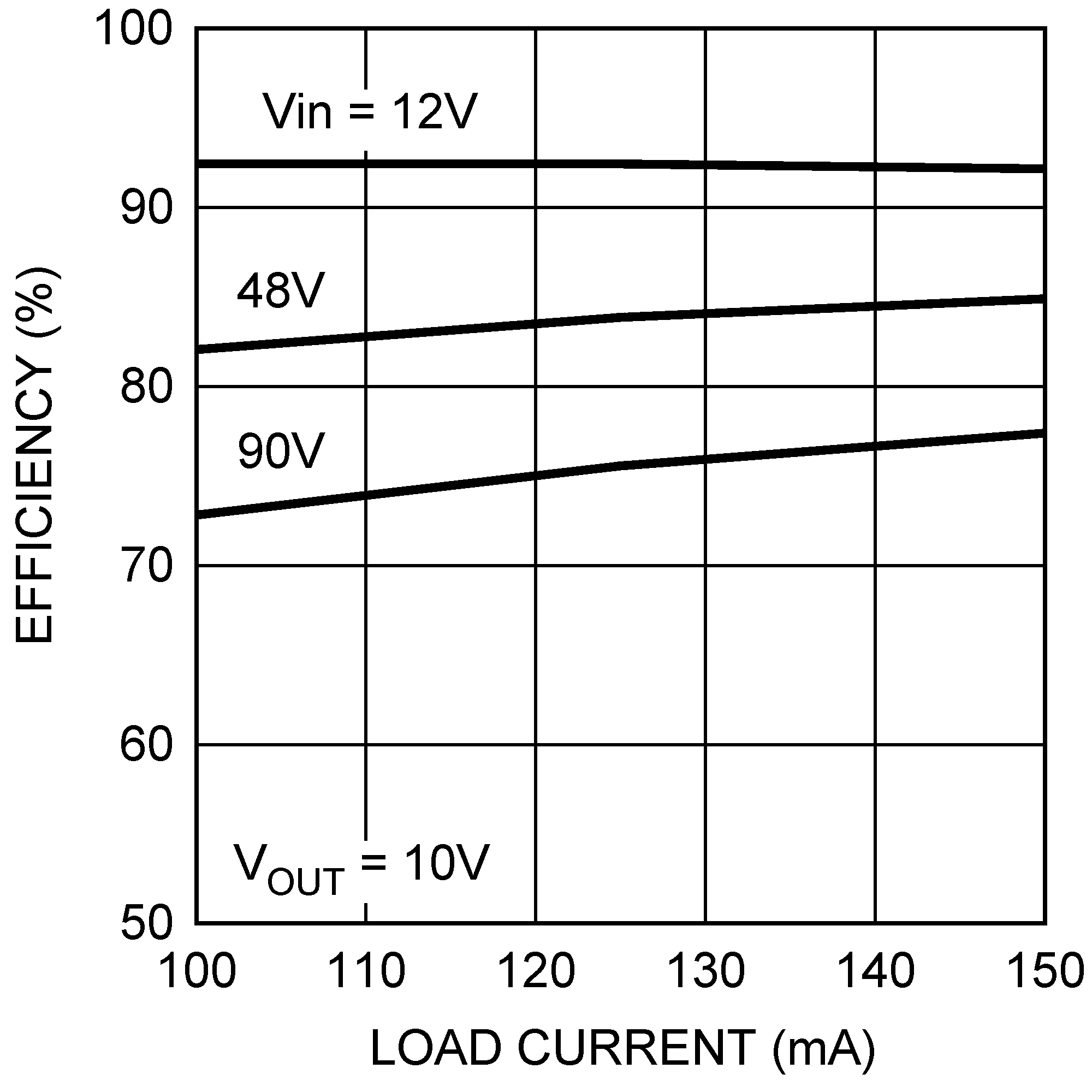 Figure 1. Efficiency vs Load Current and VIN
(Circuit of Figure 10)
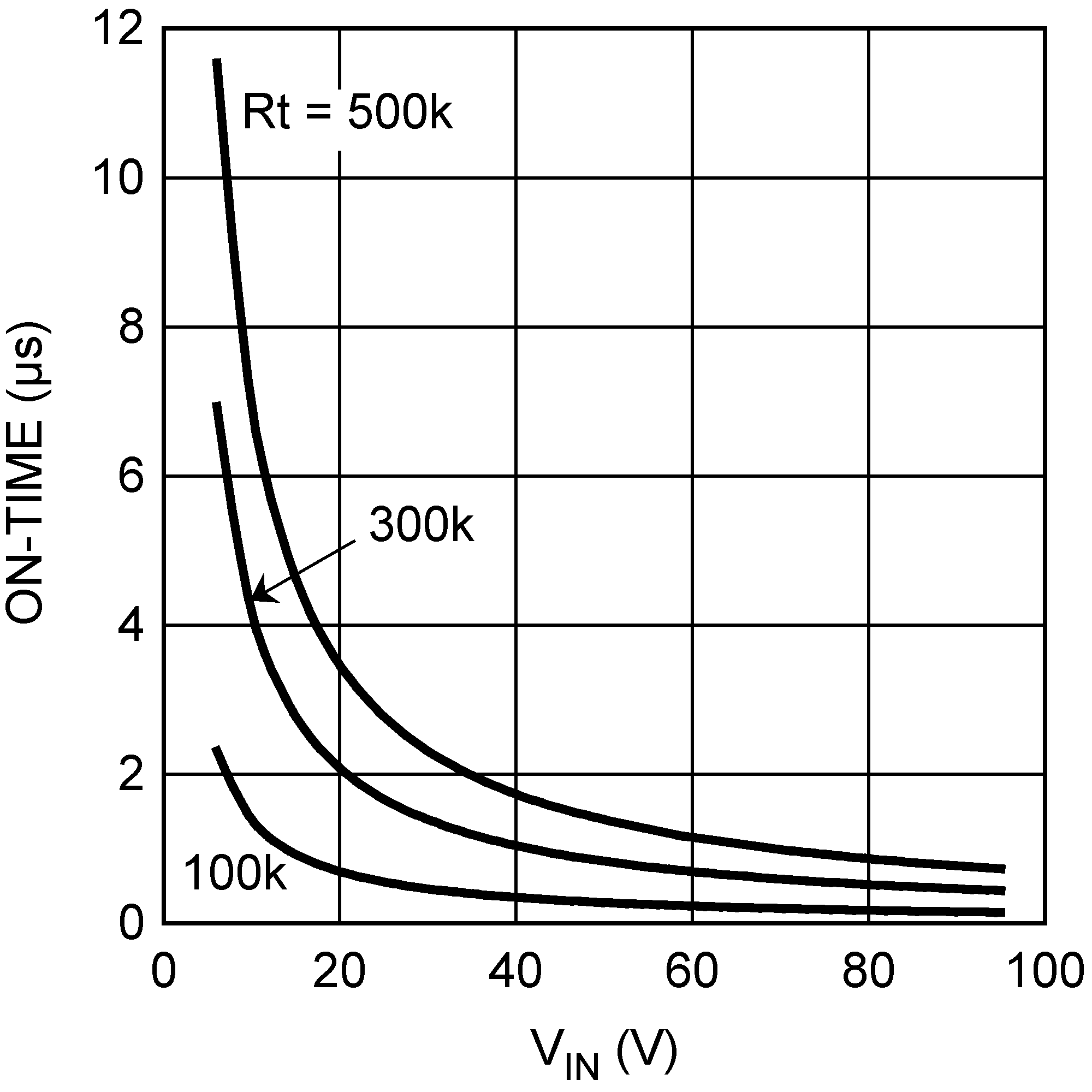 Figure 3. ON Time vs Input Voltage and RT
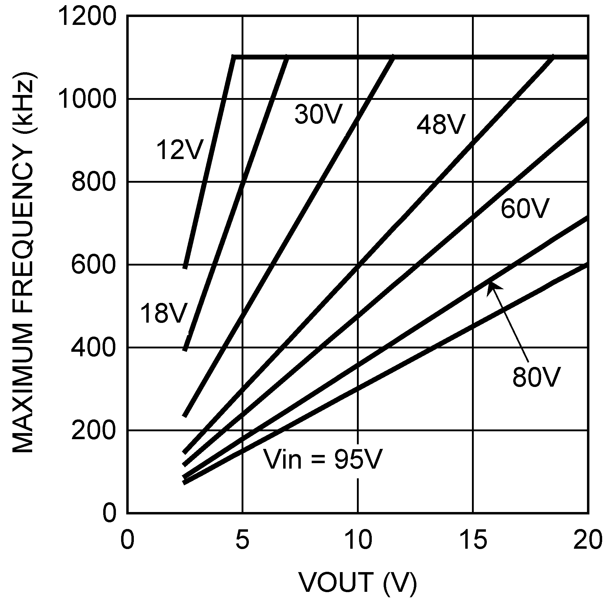 Figure 5. Maximum Frequency vs VOUT and VIN
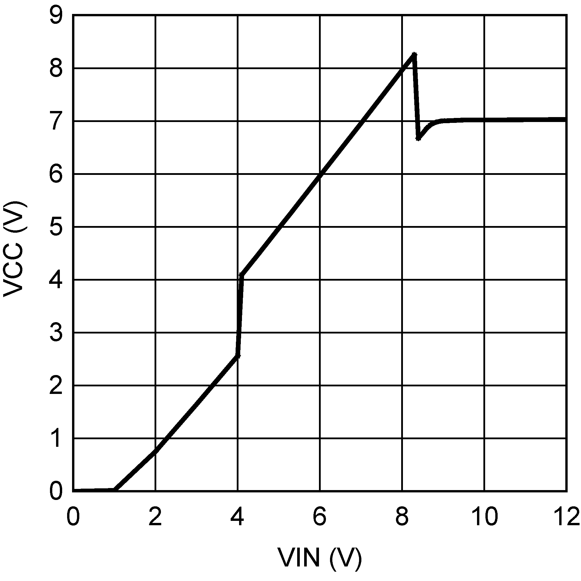 Figure 2. VCC vs VIN
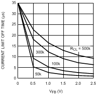 Figure 4. Current Limit OFF Time vs VFB and RCL
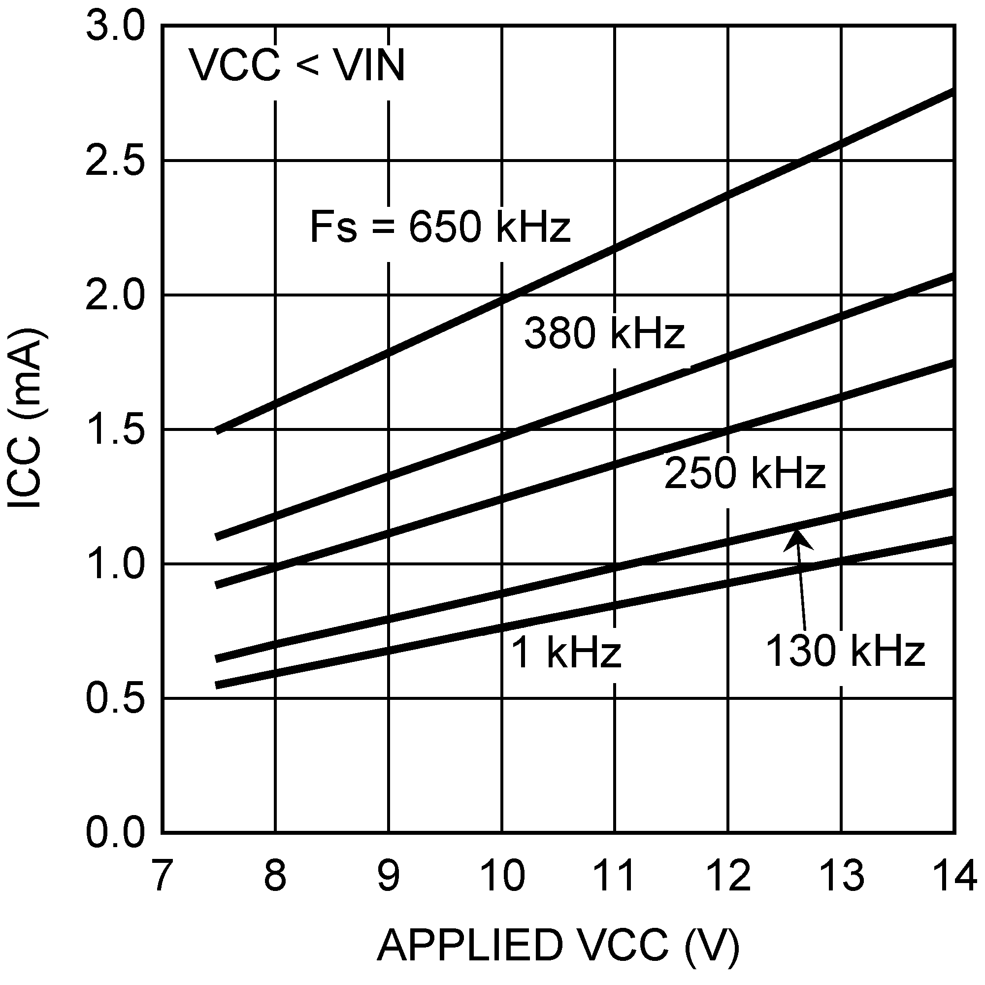 Figure 6. ICC Current vs Applied VCC Voltage