ZHCSE17B July 2015 – November 2017 LM43601-Q1
PRODUCTION DATA.
- 1 特性
- 2 应用
- 3 说明
- 4 修订历史记录
- 5 Pin Configuration and Functions
- 6 Specifications
-
7 Detailed Description
- 7.1 Overview
- 7.2 Functional Block Diagram
- 7.3
Feature Description
- 7.3.1 Fixed Frequency Peak Current Mode Controlled Step-Down Regulator
- 7.3.2 Light Load Operation
- 7.3.3 Adjustable Output Voltage
- 7.3.4 ENABLE Pin
- 7.3.5 VCC, UVLO and BIAS
- 7.3.6 Soft Start and Voltage Tracking (SS/TRK)
- 7.3.7 Switching Frequency (RT) and Synchronization (SYNC)
- 7.3.8 Minimum ON-Time, Minimum OFF-Time and Frequency Foldback at Drop-Out Conditions
- 7.3.9 Internal Compensation and CFF
- 7.3.10 Bootstrap Voltage (BOOT)
- 7.3.11 Power Good (PGOOD)
- 7.3.12 Overcurrent and Short-Circuit Protection
- 7.3.13 Thermal Shutdown
- 7.4 Device Functional Modes
-
8 Applications and Implementation
- 8.1 Application Information
- 8.2
Typical Applications
- 8.2.1 Design Requirements
- 8.2.2
Detailed Design Procedure
- 8.2.2.1 Custom Design With WEBENCH® Tools
- 8.2.2.2 Output Voltage Set-Point
- 8.2.2.3 Switching Frequency
- 8.2.2.4 Input Capacitors
- 8.2.2.5 Inductor Selection
- 8.2.2.6 Output Capacitor Selection
- 8.2.2.7 Feed-Forward Capacitor
- 8.2.2.8 Bootstrap Capacitors
- 8.2.2.9 VCC Capacitor
- 8.2.2.10 BIAS Capacitors
- 8.2.2.11 Soft-Start Capacitors
- 8.2.2.12 Undervoltage Lockout Setpoint
- 8.2.2.13 PGOOD
- 8.2.3 Application Performance Curves
- 9 Power Supply Recommendations
- 10Layout
- 11器件和文档支持
- 12机械、封装和可订购信息
8.2 Typical Applications
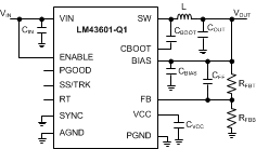
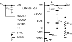
The LM43601-Q1 only requires a few external components to convert from a wide range of supply voltage to output voltage. Figure 44 shows a basic schematic when BIAS is connected to VOUT. This is recommended for VOUT ≥ 3.3 V. For VOUT< 3.3 V, connect BIAS to ground, as shown in Figure 45.
 Figure 44. LM43601-Q1 Basic Schematic for
VOUT ≥ 3.3 V, Tie BIAS to VOUT
 Figure 45. LM43601-Q1 Basic Schematic for
VOUT< 3.3 V, Tie BIAS to Ground
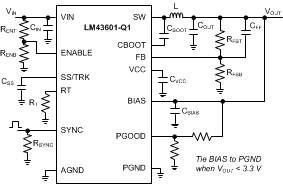
The LM43601-Q1 also integrates a full list of optional features to aid system design requirements, such as precision enable, VCC UVLO, programmable soft start, output voltage tracking, programmable switching frequency, clock synchronization and power-good indication. Each application can select the features for a more comprehensive design. A schematic with all features utilized is shown in Figure 46.
 Figure 46. LM43601-Q1 Schematic with All Features
The external components must be chosen for the application, but also the stability criteria of the device control loop. The LM43601-Q1 is optimized to work within a range of external components. The inductance and capacitance of the LC output filter must considered in conjunction, creating a double pole, responsible for the corner frequency of the converter. Table 2 can be used to simplify the output filter component selection.
Table 2. L, COUT, and CFF Typical Values
| FS (kHz) | L (µH) | COUT (µF) (1) | CFF (pF) (2)(3) | RT (kΩ) | RFBB (kΩ) (2)(3) |
|---|---|---|---|---|---|
| VOUT = 1 V | |||||
| 200 | 18 | 500 | none | 200 | 100 |
| 500 | 6.8 | 330 | none | 80.6 or open | 100 |
| 1000 | 3.3 | 180 | none | 39.2 | 100 |
| 2200 | 1.5 | 100 | none | 17.8 | 100 |
| VOUT = 3.3 V | |||||
| 200 | 47 | 220 | 44 | 200 | 442 |
| 500 | 18 | 100 | 33 | 80.6 or open | 442 |
| 1000 | 10 | 47 | 18 | 39.2 | 442 |
| 2200 | 4.7 | 27 | 12 | 17.8 | 442 |
| VOUT = 5 V | |||||
| 200 | 56 | 150 | 68 | 200 | 255 |
| 500 | 27 | 66 | 33 | 80.6 or open | 255 |
| 1000 | 15 | 33 | 22 | 39.2 | 255 |
| 2200 | 6.8 | 22 | 18 | 17.8 | 255 |
| VOUT = 12 V | |||||
| 200 | 100 | 33 | see note (4) | 200 | 90.9 |
| 500 | 47 | 22 | 47 | 80.6 or open | 90.9 |
| 1000 | 22 | 15 | 33 | 39.2 | 90.9 |