SNOS977F May 2001 – May 2016 LM397
PRODUCTION DATA.
8 Application and Implementation
NOTE
Information in the following applications sections is not part of the TI component specification, and TI does not warrant its accuracy or completeness. TI’s customers are responsible for determining suitability of components for their purposes. Customers should validate and test their design implementation to confirm system functionality.
8.1 Application Information
LM397 will typically be used to compare a single signal to a reference or two signals against each other.
8.2 Typical Application
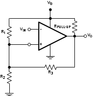
 Figure 9. Inverting Comparator With Hysteresis
8.2.1 Design Requirements
For this design example, use the parameters listed in Table 1 as the input parameters.
Table 1. Design Parameters
| DESIGN PARAMETER | EXAMPLE VALUE |
|---|---|
| Input voltage range | 0 V to VS – 1.5 V |
| Supply voltage | 5 V to 30 V |
| Logic supply voltage (RPULLUP voltage) | 5 V to 30 V |
| Output current (VLOGIC/RPULLUP) | 1 µA to 20 mA |
| Input overdrive voltage | 100 mV |
| Reference voltage | 5.5 V |
8.2.2 Detailed Design Procedure
When using TL331 in a general comparator application, determine the following:
- Input voltage range
- Minimum overdrive voltage
- Output and drive current
8.2.2.1 Input Voltage Range
When choosing the input voltage range, the input common mode voltage range (VCM) must be taken in to account. If temperature operation is above or below 25°C the VCM can range from 0 V to VS – 1.5 V. This limits the input voltage range to as high as VS – 1.5 V and as low as 0 V. Operation outside of this range can yield incorrect comparisons.
Below is a list of input voltage situation and their outcomes:
- When both IN– and IN+ are both within the common mode range:
- If IN– is higher than IN+ and the offset voltage, the output is low and the output transistor is sinking current
- If IN– is lower than IN+ and the offset voltage, the output is high impedance and the output transistor is not conducting
- When IN– is higher than common mode and IN+ is within common mode, the output is low and the output transistor is sinking current
- When IN+ is higher than common mode and IN– is within common mode, the output is high impedance and the output transistor is not conducting
- When IN– and IN+ are both higher than common mode, the output is low and the output transistor is sinking current
8.2.2.2 Minimum Overdrive Voltage
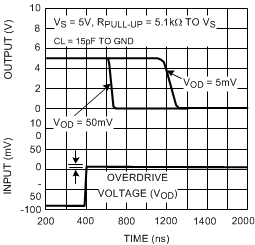
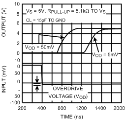
Overdrive Voltage is the differential voltage produced between the positive and negative inputs of the comparator over the offset voltage. To make an accurate comparison; the overdrive voltage should be higher than the input offset voltage. Overdrive voltage can also determine the response time of the comparator, with the response time decreasing with increasing overdrive.
8.2.2.3 Output and Drive Current
Output current is determined by the pullup resistance (RPULLUP) and VS voltage. The output current will produce a output low voltage (VOL) from the comparator. In which VOL is proportional to the output current. Use Figure 3 to determine VOL based on the output current. The output current can also effect the transient response.
8.2.3 Application Curves
 Figure 10. Response Time for Various Input Overdrives – tPHL
 Figure 11. Response Time for Various Input Overdrives – tPLH