SNVS555D January 2008 – December 2014 LM3881
PRODUCTION DATA.
- 1 Features
- 2 Applications
- 3 Description
- 4 Revision History
- 5 Pin Configuration and Functions
- 6 Specifications
- 7 Detailed Description
- 8 Application and Implementation
- 9 Power Supply Recommendations
- 10Layout
- 11Device and Documentation Support
- 12Mechanical, Packaging, and Orderable Information
8 Application and Implementation
NOTE
Information in the following applications sections is not part of the TI component specification, and TI does not warrant its accuracy or completeness. TI’s customers are responsible for determining suitability of components for their purposes. Customers should validate and test their design implementation to confirm system functionality.
8.1 Application Information
8.1.1 Open-Drain Flags Pullup
The Simple Power Sequencer contains three open-drain output flags which need to be pulled up for proper operation. 100-kΩ resistors can be used as pullup resistors.
8.1.2 Enable the Device
See Enable Circuit.
8.1.3 Timing Adjust
See Adjustable Timing.
8.2 Typical Application
8.2.1 Simple Sequencing of Three Power Supplies
The Simple Power Sequencer is used to implement a power-up (1 - 2 - 3) and power-down (3 - 2 - 1) sequence of three power supplies.
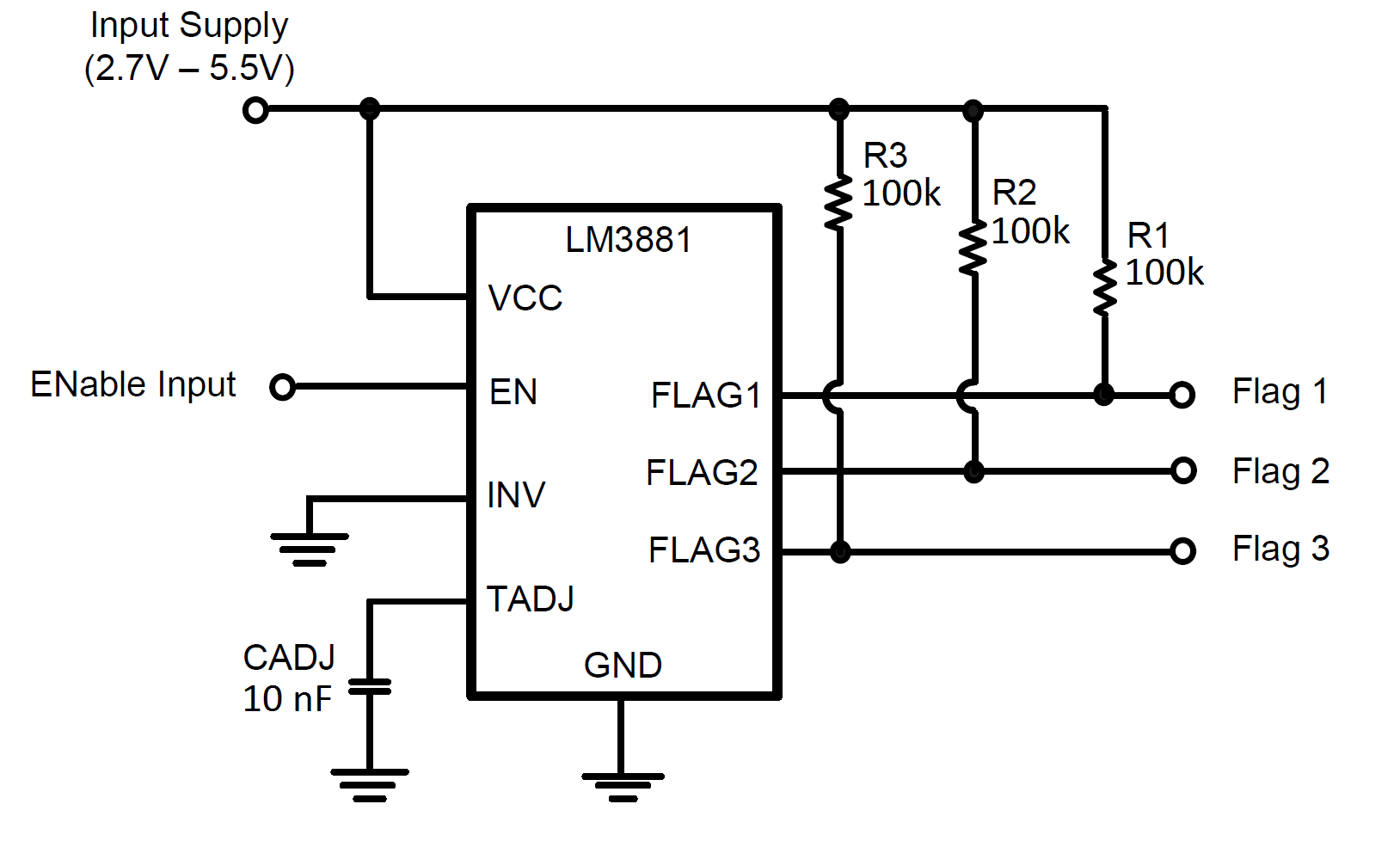 Figure 18. Typical Application Circuit
8.2.1.1 Design Requirements
For this design example, use the parameters listed in Table 1 as the input parameters.
Table 1. Design Parameters
| Design Parameter | Example Value |
|---|---|
| Input Supply voltage range | 2.7 V to 5.5 V |
| Flag Output voltage, EN high | Input Supply |
| Flag Output voltage, EN low | 0 V |
| Flag Timing Delay, TD1 | 10.8 ms - 12.0 ms |
| Flag Timing Delay, TD2 and TD3 | 9.6 ms |
| Power-Up Sequence | 1 - 2 - 3 |
| Power-Down Sequence | 3 - 2 - 1 |
8.2.1.2 Detailed Design Procedure
Table 2. Evaluation Board Bill of Materials
| Ref Des | Description | Case Size | Manufacturer | Manufacturer P/N |
|---|---|---|---|---|
| U1 | LM3881 Sequencer | MSOP-8 | Texas Instruments | LM388 |
| R1 | 100 kΩ | 0603 | Vishay Dale | CRCW06031003F-e3 |
| R2 | 100 kΩ | 0603 | Vishay Dale | CRCW06031003F-e3 |
| R3 | 100 kΩ | 0603 | Vishay Dale | CRCW06031003F-e3 |
| CADJ | 10 nF ±10% X7R 16 V | 0603 | Murata | GRM188R71C103KA01 |
A timing capacitor of CADJ = 10 nF generates typical time delays TD2 and TD3 of 9.6 ms and TD1 of between
10.8 ms and 12.0 ms. The INV pin is tied to GND so that the output flags are active high. See Adjustable Timing for calculating the value for CADJ.
8.2.1.3 Application Curves
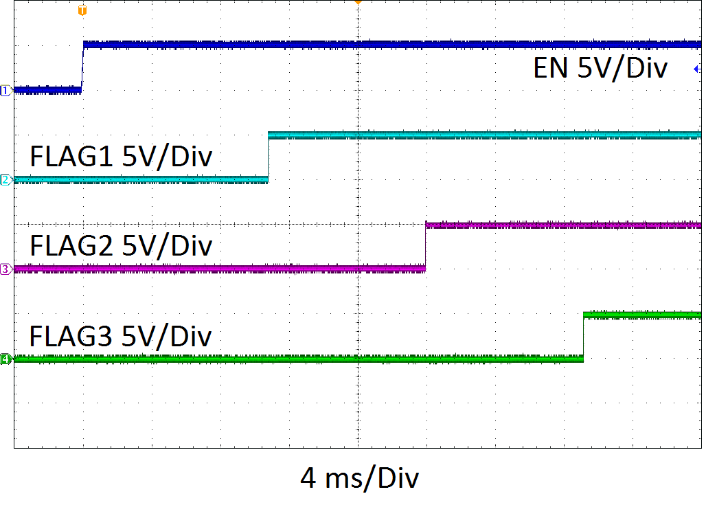 Figure 19. Power-Up Sequence, CADJ = 10 nF
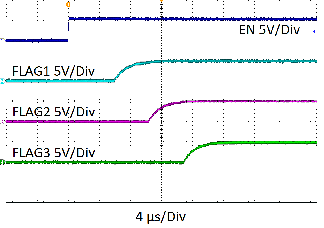 Figure 21. Power-Up Sequence, TADJ Open
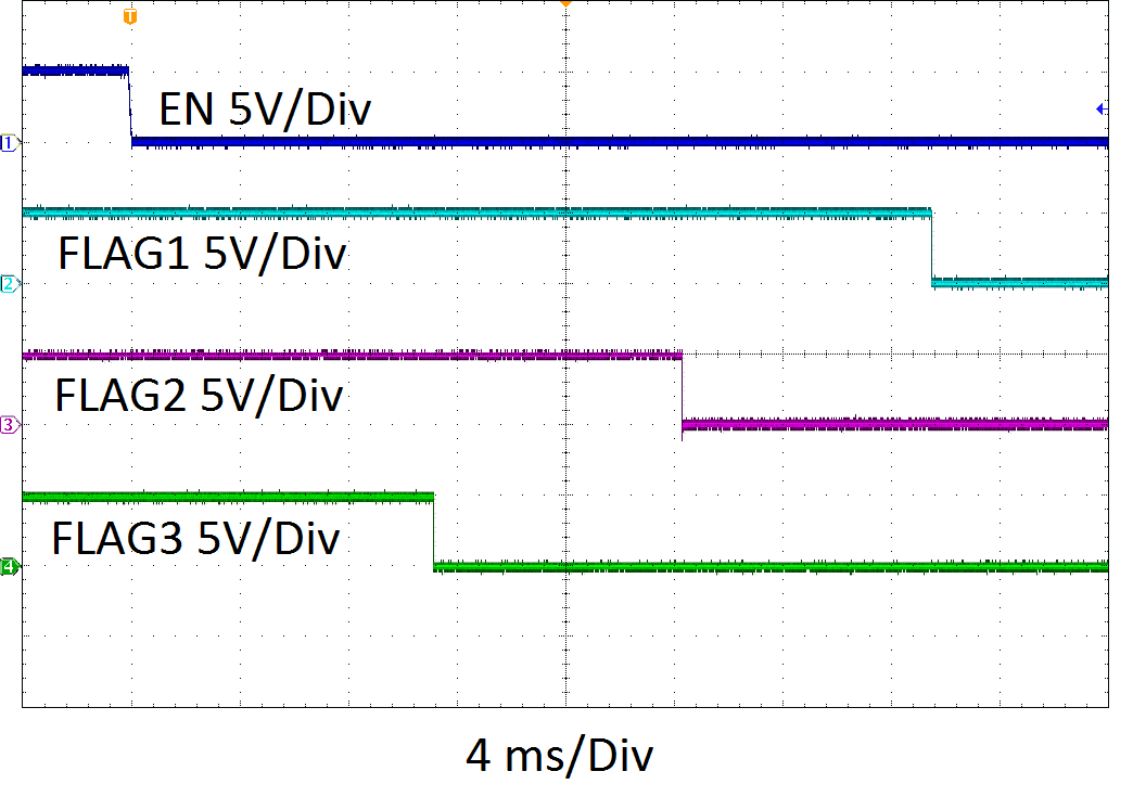 Figure 20. Power-Down Sequence, CADJ = 10 nF
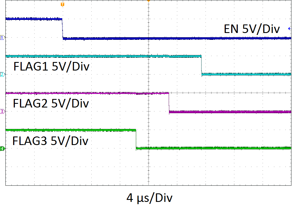 Figure 22. Power-Down Sequence, TADJ Open
8.2.2 Sequencing Using Independent Flag Supply
For applications requiring a flag output voltage that is different from the VCC, a separate Flag Supply may be used to pullup the open-drain outputs of the Simple Power Sequencer. This is useful when interfacing the flag outputs with inputs that require a different voltage than VCC. The designer must ensure the Flag Supply voltage is within the range specified in the Recommended Operating Conditions.
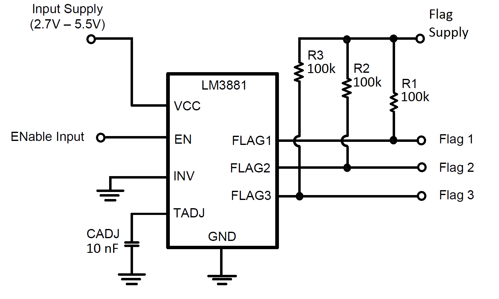 Figure 23. Sequencing Using Independent Flag Supply