SNVS834 August 2014 LM3631
PRODUCTION DATA.
- 1 Features
- 2 Applications
- 3 Description
- 4 Revision History
- 5 Device Comparison Table
- 6 Pin Configuration and Functions
- 7 Specifications
-
8 Detailed Description
- 8.1 Overview
- 8.2 Functional Block Diagram
- 8.3 Features Description
- 8.4 Device Functional Modes
- 8.5 Programming
- 8.6 Register Maps
- 9 Application and Implementation
- 10Power Supply Recommendations
- 11Layout
- 12Device and Documentation Support
- 13Mechanical, Packaging, and Orderable Information
6 Pin Configuration and Functions
DSBGA
24 BUMPS
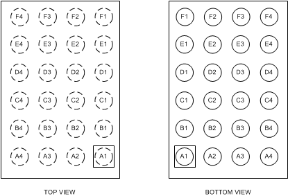
Pin Functions
| PIN | DESCRIPTION | |
|---|---|---|
| NUMBER | NAME | |
| A1 | CP_VNEG | Negative LCD bias supply voltage. Can be left unconnected if charge pump is disabled. |
| A2 | C2 | Inverting charge pump flying capacitor negative pin. Can be left unconnected if charge pump is disabled. |
| A3 | PGND | Power ground connection for boost converters and charge pump. |
| A4 | C1 | Inverting charge pump flying capacitor positive pin. Can be left unconnected if charge pump is disabled. |
| B1 | LDO_OREF | LDO_OREF output voltage. Can be left unconnected if LDO is disabled. |
| B2 | PWM | PWM input for brightness control. Must be connected to GND if not used. |
| B3 | SDA | Serial data connection for I2C-compatible interface. Must be pulled high to VDDIO if not used. |
| B4 | BST_OUT | LCD bias boost output voltage. Internally connected to the input of CP_VNEG, LDO_VPOS, and LDO_OREF. |
| C1 | LDO_VPOS | Positive LCD bias supply rail. Can be left unconnected if LDO is disabled. |
| C2 | LDO_CONT | Positive supply voltage for display panel controller. Can be left unconnected if disabled. |
| C3 | SCL | Serial clock connection for I2C-compatible interface. Must be pulled high to VDDIO if not used. |
| C4 | BST_SW | LCD bias boost switch pin. |
| D1 | AGND | Analog ground connection for control circuitry. |
| D2 | OTP_SEL | Default setting selection. Must be tied to GND or to VDDIO. |
| D3 | FLAG | Programmable interrupt flag. Open drain output. Can be left unconnected if not used. |
| D4 | GND_BST_SW | LCD bias boost and inverting charge pump ground connection. |
| E1 | LED2 | Input pin to internal LED current sink 2. Can be left unconnected if not used. |
| E2 | LCD_EN | LCD enable input. Logic high turns on LCD bias voltages and backlight per sequencing settings. |
| E3 | nRST | Active low reset input. |
| E4 | VIN | Input voltage connection. Connect to 2.7-V to 5-V supply voltage. |
| F1 | LED1 | Input pin to internal LED current sink 1. Can be left unconnected if not used. |
| F2 | VOUT | Backlight boost output voltage. Output capacitor is connected to this pin. |
| F3 | SW | Backlight boost switch pin. |
| F4 | GND_SW | Backlight boost ground connection. |