ZHCSE58C April   2012  – September 2015 LM3533

PRODUCTION DATA.  

  1. 特性
  2. 应用范围
  3. 说明
  4. 修订历史记录
  5. Pin Configuration and Functions
  6. Specifications
    1. 6.1 Absolute Maximum Ratings
    2. 6.2 ESD Ratings
    3. 6.3 Recommended Operating Conditions
    4. 6.4 Thermal Information
    5. 6.5 Electrical Characteristics
    6. 6.6 I2C Timing Requirements
    7. 6.7 Typical Characteristics
  7. Detailed Description
    1. 7.1 Overview
    2. 7.2 Functional Block Diagram
    3. 7.3 Feature Description
      1. 7.3.1 Control Bank Mapping
        1. 7.3.1.1 High-Voltage Control Banks (A/B)
        2. 7.3.1.2 Low-Voltage Control Banks (C, D, E, And F)
      2. 7.3.2 Pattern Generator
      3. 7.3.3 Ambient Light Sensor Interface
      4. 7.3.4 PWM Input
      5. 7.3.5 HWEN Input
      6. 7.3.6 Thermal Shutdown
    4. 7.4 Device Functional Modes
      1. 7.4.1  High-Voltage Boost Converter
        1. 7.4.1.1 High-Voltage Current Sinks (HVLED1 And HVLED2)
        2. 7.4.1.2 High-Voltage Current String Biasing
        3. 7.4.1.3 Boost Switching-Frequency Select
      2. 7.4.2  Integrated Charge Pump
        1. 7.4.2.1 Charge Pump Disabled
        2. 7.4.2.2 Automatic Gain
        3. 7.4.2.3 Automatic Gain (Flying Capacitor Detection)
        4. 7.4.2.4 1× Gain
        5. 7.4.2.5 2× Gain
        6. 7.4.2.6 Low-Voltage Current Sinks (LVLED1 to LVLED5)
        7. 7.4.2.7 Low-Voltage LED Biasing
      3. 7.4.3  LED Current Mapping Modes
        1. 7.4.3.1 Exponential Mapping
        2. 7.4.3.2 Linear Mapping
      4. 7.4.4  LED Current Ramping
        1. 7.4.4.1 Start-Up/Shutdown Ramp
        2. 7.4.4.2 Run-Time Ramp
      5. 7.4.5  Brightness Register Current Control
      6. 7.4.6  PWM Control
        1. 7.4.6.1 PWM Input Frequency Range
        2. 7.4.6.2 PWM Input Polarity
      7. 7.4.7  ALS Current Control
        1. 7.4.7.1 ALS Brightness Zones (Zone Boundaries)
        2. 7.4.7.2 Zone Boundary Hysteresis
        3. 7.4.7.3 Zone Target Registers (ALSM1, ALSM2, ALSM3)
        4. 7.4.7.4 PWM Input in ALS Mode
      8. 7.4.8  ALS Functional Blocks
        1. 7.4.8.1  ALS Input
        2. 7.4.8.2  Analog Output Ambient Light Sensors (ALS Gain Setting Resistors)
        3. 7.4.8.3  PWM Output Ambient Light Sensors (Internal Filtering)
        4. 7.4.8.4  Internal 8-Bit ADC
        5. 7.4.8.5  ALS Averager
        6. 7.4.8.6  Initializing the ALS
        7. 7.4.8.7  ALS Algorithms
        8. 7.4.8.8  ALS Rules
        9. 7.4.8.9  Direct ALS Control
        10. 7.4.8.10 Up-Only Control
        11. 7.4.8.11 Down-Delay Control
      9. 7.4.9  Pattern Generator
        1. 7.4.9.1 Delay Time
        2. 7.4.9.2 Rise Time
        3. 7.4.9.3 Fall Time
        4. 7.4.9.4 High Period
        5. 7.4.9.5 Low Period
        6. 7.4.9.6 Low-Level Brightness
        7. 7.4.9.7 High-Level Brightness
        8. 7.4.9.8 ALS Controlled Pattern Current
        9. 7.4.9.9 Interrupt Output Mode
      10. 7.4.10 Fault Flags/Protection Features
        1. 7.4.10.1 Open LED String (HVLED)
        2. 7.4.10.2 Shorted LED String (HVLED)
        3. 7.4.10.3 Open LED (LVLED)
        4. 7.4.10.4 Shorted LED (LVLED)
        5. 7.4.10.5 Overvoltage Protection (Inductive Boost)
        6. 7.4.10.6 Current Limit (Inductive Boost)
        7. 7.4.10.7 Current Limit (Charge Pump)
    5. 7.5 Programming
      1. 7.5.1 I2C-Compatible Interface
        1. 7.5.1.1 Start and Stop Conditions
        2. 7.5.1.2 I2C-Compatible Address
        3. 7.5.1.3 Transferring Data
    6. 7.6 Register Maps
      1. 7.6.1 LM3533 Register Descriptions
        1. 7.6.1.1 Pattern Generator Registers
  8. Application and Implementation
    1. 8.1 Application Information
    2. 8.2 Typical Application
      1. 8.2.1 Design Requirements
      2. 8.2.2 Detailed Design Procedure
        1. 8.2.2.1 Boost Converter Maximum Output Power (Boost)
        2. 8.2.2.2 Peak Current Limited
        3. 8.2.2.3 Output Voltage Limited
        4. 8.2.2.4 Maximum Output Power (Charge Pump)
      3. 8.2.3 Application Curves
  9. Power Supply Recommendations
  10. 10Layout
    1. 10.1 Layout Guidelines
      1. 10.1.1 Boost
        1. 10.1.1.1 Boost Output Capacitor Selection and Placement
        2. 10.1.1.2 Schottky Diode Placement
        3. 10.1.1.3 Inductor Placement
        4. 10.1.1.4 Boost Input Capacitor Selection and Placement
      2. 10.1.2 Charge Pump
        1. 10.1.2.1 Flying Capacitor (CP)
        2. 10.1.2.2 Output Capacitor (CPOUT)
        3. 10.1.2.3 Charge Pump Input Capacitor Placement
    2. 10.2 Layout Example
  11. 11器件和文档支持
    1. 11.1 器件支持
      1. 11.1.1 Third-Party Products Disclaimer
    2. 11.2 相关文档 
    3. 11.3 社区资源
    4. 11.4 商标
    5. 11.5 静电放电警告
    6. 11.6 Glossary
  12. 12机械、封装和可订购信息

封装选项

机械数据 (封装 | 引脚)
散热焊盘机械数据 (封装 | 引脚)
订购信息

5 Pin Configuration and Functions

YFQ Package
20-Pin DSBGA
Top View
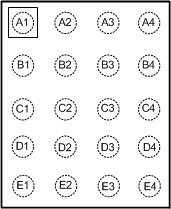
LM3533 30135702.gif

Pin Functions

PIN TYPE DESCRIPTION
NO. NAME
A1 C− OUT Integrated charge pump flying capacitor negative terminal. Connect a 1-µF ceramic capacitor from C+ to C−.
A2 C+ OUT Integrated charge pump flying capacitor positive terminal. Connect a 1-µF ceramic capacitor from C+ to C−.
A3 CPOUT OUT Integrated charge pump output terminal. Bypass CPOUT to GND with a 1-µF ceramic capacitor.
A4 IN IN Input voltage connection. Bypass IN to GND with a minimum 2.2-µF ceramic capacitor.
B1 SCL IN Serial clock connection for I2C-compatible interface.
B2 SDA I/O Serial data connection for I2C-compatible interface.
B3 OVP IN Overvoltage sense Input. Connect OVP to the positive terminal of the inductive boost's output capacitor (COUT).
B4 GND GND Ground
C1 HVLED1 IN Input pin to high-voltage current sink 1 (40 V maximum). The boost converter regulates the minimum of HVLED1 and HVLED2 to 0.4 V.
C2 INT OUT ALS interrupt output (INT). When INT mode is enabled this pin becomes an open-drain output that pulls low when the ALS changes zones. On power-up, INT mode is disabled and is high impedance and must be tied high or low.
C3 PWM IN PWM brightness control input for CABC operation. PWM is a high-impedance input and cannot be left floating.
C4 SW IN Drain connection for the internal NFET. Connect SW to the junction of the inductor and the Schottky diode anode.
D1 HVLED2 IN Input pin high-voltage current sink 2 (40 V maximum). The boost converter regulates the minimum of HVLED1 and HVLED2 to 0.4 V.
D2 ALS IN Ambient light sensor input.
D3 HWEN IN Hardware enable input. Drive this pin high to enable the device. Drive this pin low to force the device into a low power shutdown. HWEN is a high-impedance input and cannot be left floating.
D4 LVLED5 IN Low-voltage current sink 5
E1 LVLED1 IN Low-voltage current sink 1
E2 LVLED2 IN Low-voltage current sink 2
E3 LVLED3 IN Low-voltage current sink 3
E4 LVLED4 IN Low-voltage current sink 4