ZHCSEC6B March 2012 – October 2015 LM3492HC , LM3492HC-Q1
PRODUCTION DATA.
- 1 特性
- 2 应用
- 3 说明
- 4 修订历史记录
- 5 说明(继续)
- 6 Pin Configuration and Functions
- 7 Specifications
-
8 Detailed Description
- 8.1 Overview
- 8.2 Functional Block Diagram
- 8.3 Feature Description
- 8.4 Device Functional Modes
- 8.5 Programming
- 9 Application and Implementation
- 10Power Supply Recommendations
- 11Layout
- 12器件和文档支持
- 13机械、封装和可订购信息
11 Layout
11.1 Layout Guidelines
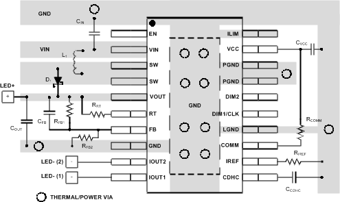
The layout of the printed-circuit-board is critical to optimize the performance of the LM3492HC device application circuit. In general, external components should be placed as close to the device and each other as possible to make copper traces short and direct. In particular, components of the boost converter CIN, L1, D1, COUT, and the LM3492HC device should be closed. Also, the output feedback capacitor CFB should be closed to the output capacitor COUT. The ground plane connecting the GND, PGND, and LGND pins and the exposed pad of the device and the ground connection of the CIN and COUT should be placed on the same copper layer.
Good heat dissipation helps optimize the performance of the device. The ground plane should be used to connect the exposed pad of the device , which is internally connected to the device die substrate. The area of the ground plane should be extended as much as possible on the same copper layer around the device. Using numerous vias beneath the exposed pad to dissipate heat of the device to another copper layer is also a good practice.
11.2 Layout Example
 Figure 32. Layout Recommendation