SNVS089O July 2000 – July 2015 LM3488
PRODUCTION DATA.
- 1 Features
- 2 Applications
- 3 Description
- 4 Revision History
- 5 Pin Configuration and Functions
- 6 Specifications
- 7 Detailed Description
-
8 Application and Implementation
- 8.1 Application Information
- 8.2
Typical Applications
- 8.2.1
Boost Converter
- 8.2.1.1 Design Requirements
- 8.2.1.2
Detailed Design Procedure
- 8.2.1.2.1 Custom Design with WEBENCH Tools
- 8.2.1.2.2 Power Inductor Selection
- 8.2.1.2.3 Programming the Output Voltage
- 8.2.1.2.4 Setting the Current Limit
- 8.2.1.2.5 Current Limit with External Slope Compensation
- 8.2.1.2.6 Power Diode Selection
- 8.2.1.2.7 Power MOSFET Selection
- 8.2.1.2.8 Input Capacitor Selection
- 8.2.1.2.9 Output Capacitor Selection
- 8.2.1.3 Application Curve
- 8.2.2 Designing SEPIC Using LM3488
- 8.2.1
Boost Converter
- 9 Power Supply Recommendations
- 10Layout
- 11Device and Documentation Support
- 12Mechanical, Packaging, and Orderable Information
6 Specifications
6.1 Absolute Maximum Ratings (1)
| MIN | MAX | UNIT | ||
|---|---|---|---|---|
| Input voltage | 45 | V | ||
| FB pin voltage | –0.4 < VFB | VFB < 7 | V | |
| FA/SYNC/SD pin voltage | –0.4 < VFA/SYNC/SD | VFA/SYNC/SD < 7 | V | |
| Peak driver output current (< 10 µs) | 1 | A | ||
| Power dissipation | Internally Limited | |||
| Junction temperature | 150 | °C | ||
| Lead temperature | Vapor Phase (60 s) | 215 | °C | |
| Infared (15 s) | 260 | °C | ||
| DR pin voltage | −0.4 ≤ VDR | VDR ≤ 8 | V | |
| ILIM pin voltage | 600 | mV | ||
6.2 ESD Ratings : LM3488
| MIN | MAX | UNIT | |||
|---|---|---|---|---|---|
| V(ESD) | Electrostatic discharge | Human body model (HBM), per ANSI/ESDA/JEDEC JS-001, all pins(1) | –2000 | 2000 | V |
| Charged device model (CDM), per JEDEC specification JESD22-C101, all pins(2) | –750 | 750 | |||
(1) JEDEC document JEP155 states that 500-V HBM allows safe manufacturing with a standard ESD control process.
(2) JEDEC document JEP157 states that 250-V CDM allows safe manufacturing with a standard ESD control process.
6.3 ESD Ratings: LM3488-Q1
| MIN | MAX | UNIT | ||||
|---|---|---|---|---|---|---|
| V(ESD) | Electrostatic discharge | Human body model (HBM), per AEC Q100-002(1) | –2000 | 2000 | V | |
| Charged device model (CDM), per AEC Q100-011 | Corner pins (1, 4, 5, and 8) | –750 | 750 | |||
| Other pins | –750 | 750 | ||||
(1) AEC Q100-002 indicates HBM stressing is done in accordance with the ANSI/ESDA/JEDEC JS-001 specification.
6.4 Recommended Operating Conditions
| MIN | MAX | UNIT | |
|---|---|---|---|
| Supply Voltage | 2.97 ≤ VIN | VIN ≤ 40 | V |
| Junction Temperature Range | −40 ≤ TJ | TJ ≤ 125 | °C |
| Switching Frequency | 100 ≤ FSW | FSW ≤ 1 | kHz/MHz |
6.5 Thermal Information
| THERMAL METRIC(1) | LM3488, LM3488-Q1 |
UNIT | |
|---|---|---|---|
| DGK | |||
| 8 PINS | |||
| RθJA | Junction-to-ambient thermal resistance | 160 | °C/W |
| RθJC(top) | Junction-to-case (top) thermal resistance | 50 | |
| RθJB | Junction-to-board thermal resistance | 77 | |
| ψJT | Junction-to-top characterization parameter | 4.7 | |
| ψJB | Junction-to-board characterization parameter | 76 | |
(1) For more information about traditional and new thermal metrics, see the IC Package Thermal Metrics application report, SPRA953.
6.6 Electrical Characteristics
Unless otherwise specified, VIN = 12 V, RFA = 40 kΩ, TJ = 25°C| PARAMETER | TEST CONDITIONS | MIN | TYP | MAX | UNIT | |
|---|---|---|---|---|---|---|
| VFB | Feedback Voltage | VCOMP = 1.4 V, 2.97 ≤ VIN ≤ 40 V | 1.2507 | 1.26 | 1.2753 | V |
| VCOMP = 1.4 V, 2.97 ≤ VIN ≤ 40 V, −40°C ≤ TJ ≤ 125°C | 1.24 | 1.28 | ||||
| ΔVLINE | Feedback Voltage Line Regulation | 2.97 ≤ VIN ≤ 40 V | 0.001 | %/V | ||
| ΔVLOAD | Output Voltage Load Regulation | IEAO Source/Sink | ±0.5 | %/V (max) | ||
| VUVLO | Input Undervoltage Lock-out | 2.85 | V | |||
| −40°C ≤ TJ ≤ 125°C | 2.97 | |||||
| VUV(HYS) | Input Undervoltage Lock-out Hysteresis | 170 | mV | |||
| −40°C ≤ TJ ≤ 125°C | 130 | 210 | ||||
| Fnom | Nominal Switching Frequency | RFA = 40 KΩ | 400 | kHz | ||
| RFA = 40 KΩ, −40°C ≤ TJ ≤ 125°C | 360 | 430 | ||||
| RDS1 (ON) | Driver Switch On Resistance (top) | IDR = 0.2A, VIN= 5 V | 16 | Ω | ||
| RDS2 (ON) | Driver Switch On Resistance (bottom) | IDR = 0.2A | 4.5 | Ω | ||
| VDR (max) | Maximum Drive Voltage Swing(3) | VIN < 7.2 V | VIN | V | ||
| VIN ≥ 7.2 V | 7.2 | |||||
| Dmax | Maximum Duty Cycle(4) | 100% | ||||
| Tmin (on) | Minimum On Time | 325 | nsec | |||
| −40°C ≤ TJ ≤ 125°C | 230 | 550 | ||||
| ISUPPLY | Supply Current (switching) | See (6) | 2.7 | mA | ||
| See (6), −40°C ≤ TJ ≤ 125°C | 3.0 | |||||
| IQ | Quiescent Current in Shutdown Mode | VFA/SYNC/SD = 5 V(7), VIN = 5 V | 5 | µA | ||
| VFA/SYNC/SD = 5 V(7), VIN = 5 V, −40°C ≤ TJ ≤ 125°C | 7 | |||||
| VSENSE | Current Sense Threshold Voltage | VIN = 5 V | 135 | 156 | 180 | mV |
| VIN = 5 V, −40°C ≤ TJ ≤ 125°C | 125 | 190 | ||||
| VSC | Short-Circuit Current Limit Sense Voltage | VIN = 5 V | 343 | mV | ||
| VIN = 5 V, −40°C ≤ TJ ≤ 125°C | 250 | 415 | ||||
| VSL | Internal Compensation Ramp Voltage | VIN = 5 V | 92 | mV | ||
| VIN = 5 V, −40°C ≤ TJ ≤ 125°C | 52 | 132 | ||||
| VSL ratio | VSL/VSENSE | 0.30 | 0.49 | 0.70 | ||
| VOVP | Output Overvoltage Protection (with respect to feedback voltage) (5) | VCOMP = 1.4 V | 32 | 50 | 78 | mV |
| VCOMP = 1.4 V, −40°C ≤ TJ ≤ 125°C | 25 | 85 | ||||
| VOVP(HYS) | Output Over-Voltage Protection Hysteresis(5) | VCOMP = 1.4 V | 60 | mV | ||
| VCOMP = 1.4 V, −40°C ≤ TJ ≤ 125°C | 20 | 110 | ||||
| Gm | Error Ampifier Transconductance | VCOMP = 1.4 V, IEAO = 100 µA (Source/Sink) | 600 | 800 | 1000 | µmho |
| VCOMP = 1.4 V, IEAO = 100 µA (Source/Sink), −40°C ≤ TJ ≤ 125°C | 365 | 1265 | ||||
| AVOL | Error Amplifier Voltage Gain | VCOMP = 1.4 V, IEAO = 100 µA (Source/Sink) | 38 | V/V | ||
| VCOMP = 1.4 V, IEAO = 100 µA (Source/Sink), −40°C ≤ TJ ≤ 125°C | 26 | 44 | ||||
| IEAO | Error Amplifier Output Current (Source/ Sink) | Source, VCOMP = 1.4 V, VFB = 0 V | 80 | 110 | 140 | µA |
| Source, VCOMP = 1.4 V, VFB = 0 V, −40°C ≤ TJ ≤ 125°C | 50 | 180 | ||||
| Sink, VCOMP = 1.4 V, VFB = 1.4 V | −100 | −140 | −180 | µA | ||
| Sink, VCOMP = 1.4 V, VFB = 1.4 V, −40°C ≤ TJ ≤ 125°C | −85 | −185 | ||||
| VEAO | Error Amplifier Output Voltage Swing | Upper Limit: VFB = 0 V, COMP Pin = Floating | 2.2 | V | ||
| Upper Limit: VFB = 0 V, COMP Pin = Floating, −40°C ≤ TJ ≤ 125°C | 1.8 | 2.4 | ||||
| Lower Limit: VFB = 1.4 V | 0.56 | V | ||||
| Lower Limit: VFB = 1.4 V, −40°C ≤ TJ ≤ 125°C | 0.2 | 1.0 | ||||
| TSS | Internal Soft-Start Delay | VFB = 1.2 V, VCOMP = Floating | 4 | ms | ||
| Tr | Drive Pin Rise Time | Cgs = 3000 pf, VDR = 0 to 3 V | 25 | ns | ||
| Tf | Drive Pin Fall Time | Cgs = 3000 pf, VDR = 0 to 3 V | 25 | ns | ||
| VSD | Shutdown and Synchronization signal threshold (2) | Output = High | 1.27 | V | ||
| Output = High, −40°C ≤ TJ ≤ 125°C | 1.4 | |||||
| Output = Low | 0.65 | V | ||||
| Output = Low, −40°C ≤ TJ ≤ 125°C | 0.3 | |||||
| ISD | Shutdown Pin Current | VSD = 5 V | −1 | µA | ||
| VSD = 0 V | +1 | |||||
| IFB | Feedback Pin Current | 15 | nA | |||
| TSD | Thermal Shutdown | 165 | °C | |||
| Tsh | Thermal Shutdown Hysteresis | 10 | °C |
(1) Absolute Maximum Ratings are limits beyond which damage to the device may occur. Recommended Operating Conditions are conditions under which operation of the device is intended to be functional. For specifications and test conditions, see the Electrical Characteristics.
(2) The FA/SYNC/SD pin should be pulled to VIN through a resistor to turn the regulator off.
(3) The voltage on the drive pin, VDR is equal to the input voltage when input voltage is less than 7.2 V. VDR is equal to 7.2 V when the input voltage is greater than or equal to 7.2 V.
(4) The limits for the maximum duty cycle can not be specified since the part does not permit less than 100% maximum duty cycle operation.
(5) The over-voltage protection is specified with respect to the feedback voltage. This is because the over-voltage protection tracks the feedback voltage. The over-voltage thresold can be calculated by adding the feedback voltage, VFB to the over-voltage protection specification.
(6) For this test, the FA/SYNC/SD Pin is pulled to ground using a 40K resistor .
(7) For this test, the FA/SYNC/SD Pin is pulled to 5 V using a 40K resistor.
6.7 Typical Characteristics
Unless otherwise specified, VIN = 12V, TJ = 25°C.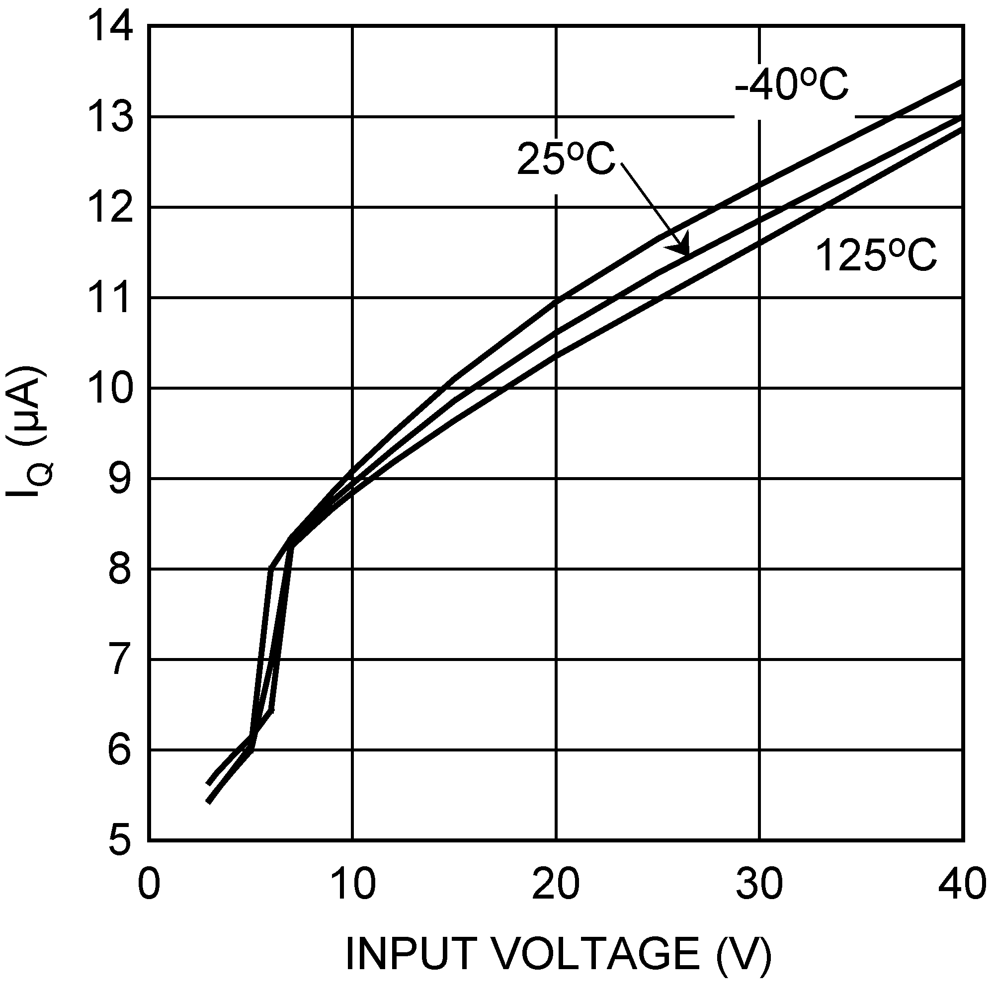 Figure 1. IQ vs Temperature & Input Voltage
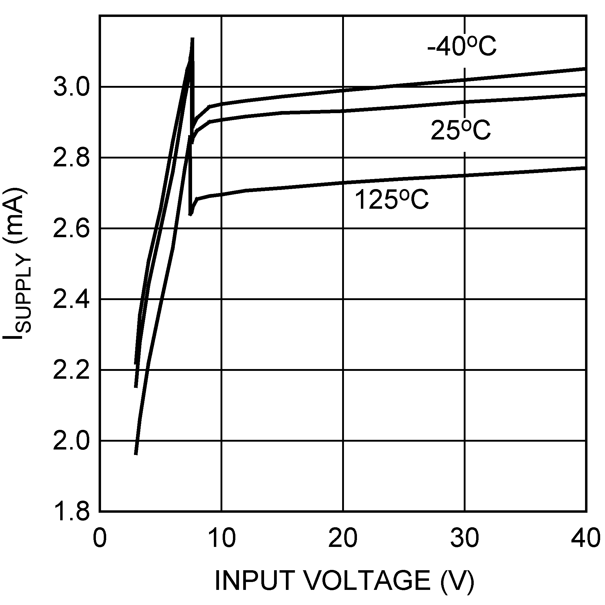 Figure 3. ISupply vs VIN
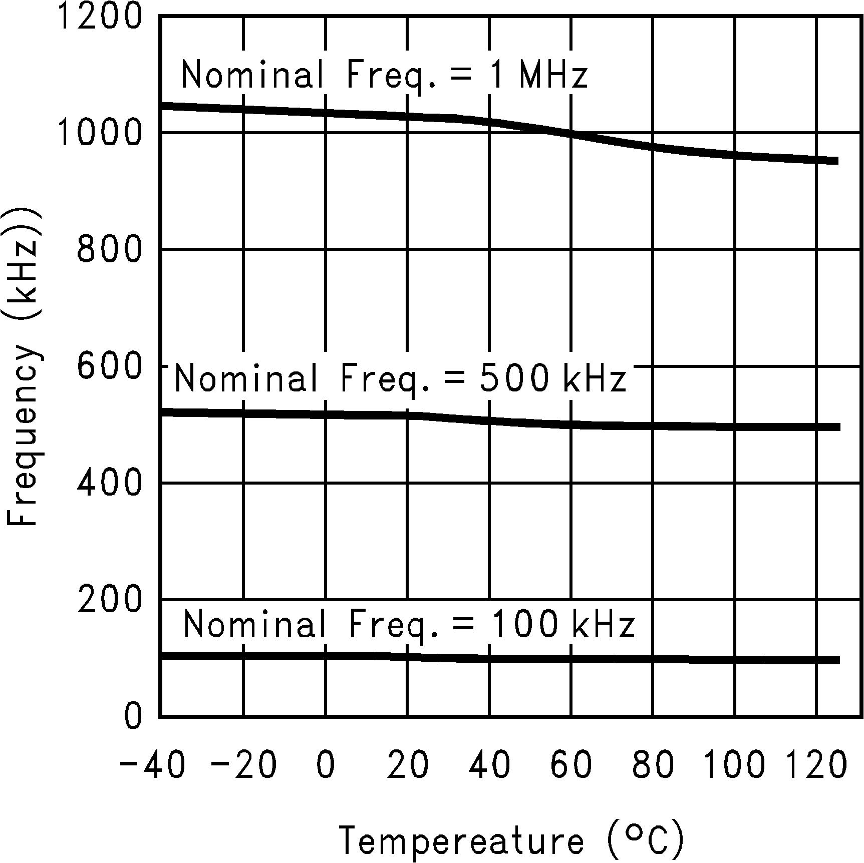 Figure 5. Frequency vs Temperature
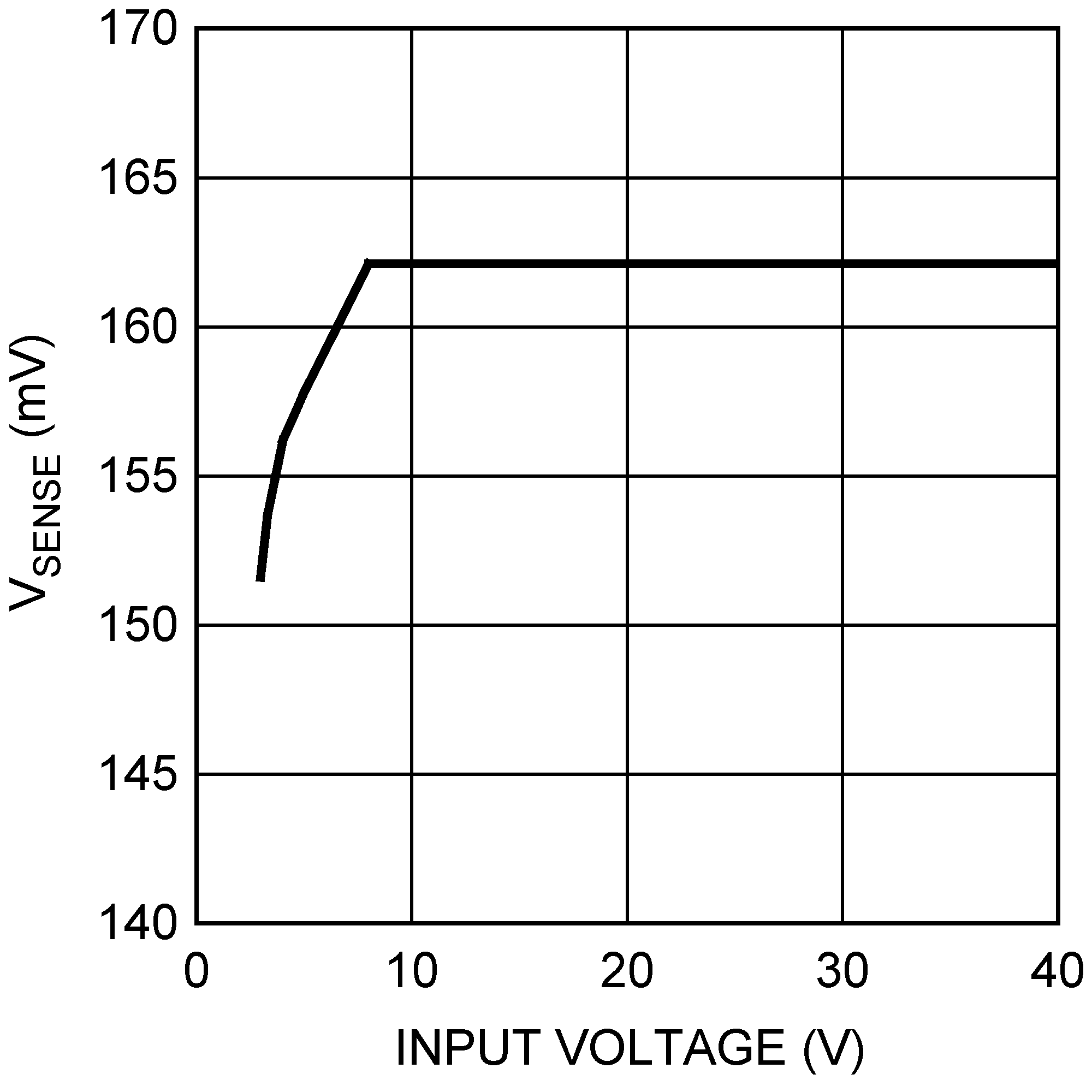 Figure 7. Current Sense Threshold vs Input Voltage
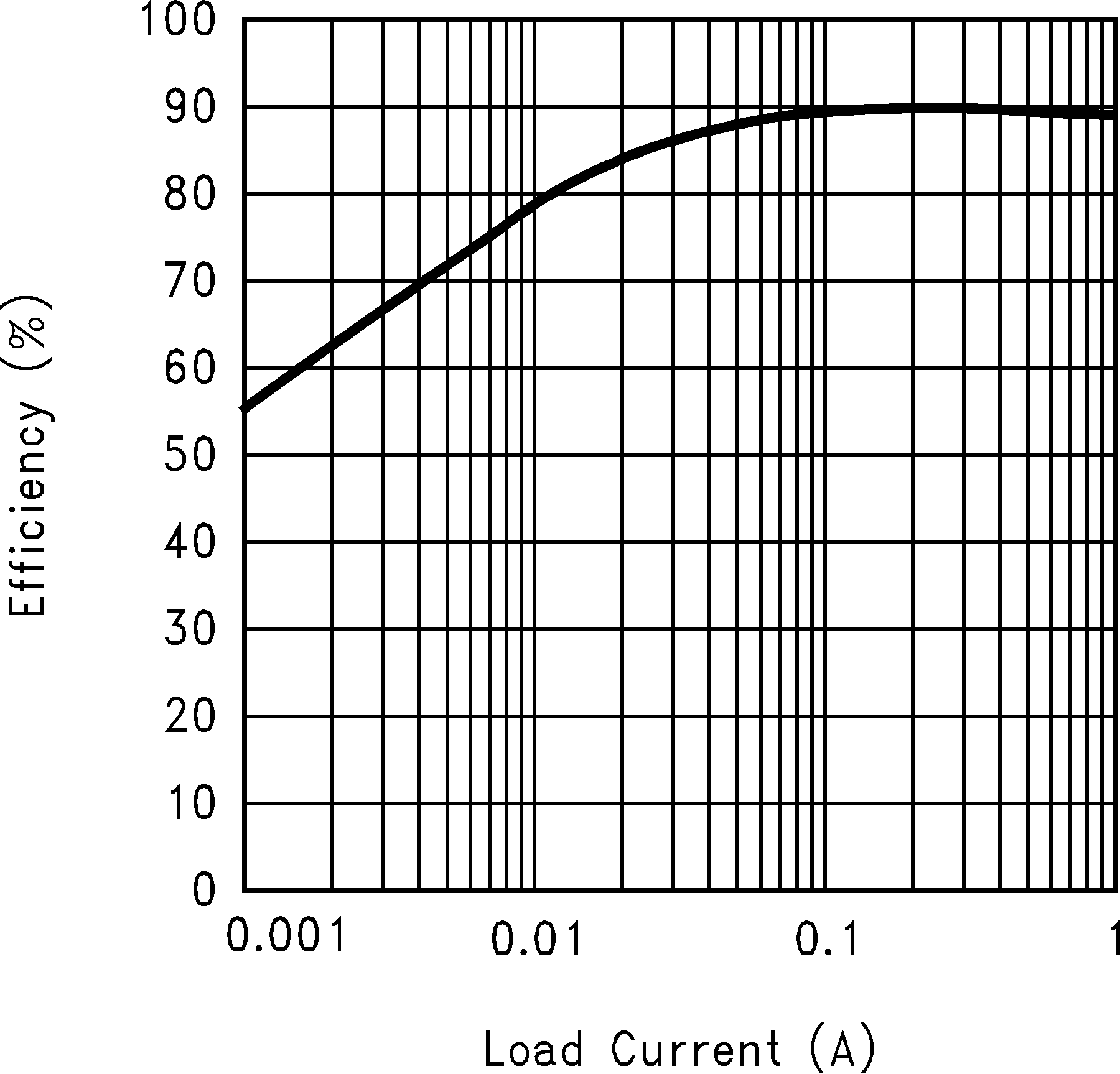 Figure 9. Efficiency vs Load Current (3.3 V In and 12 V Out)
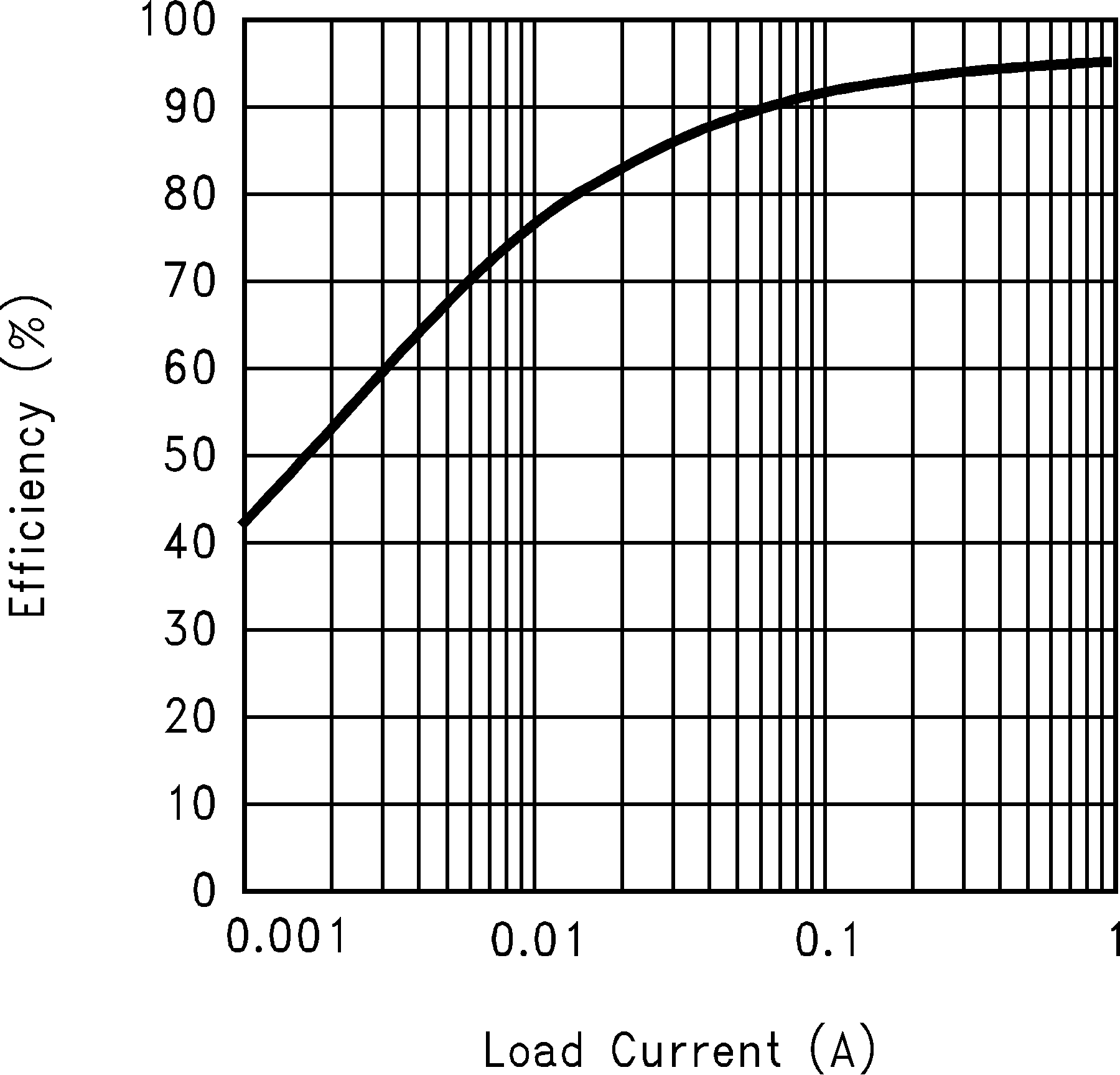 Figure 11. Efficiency vs Load Current (9 V In and 12 V Out)
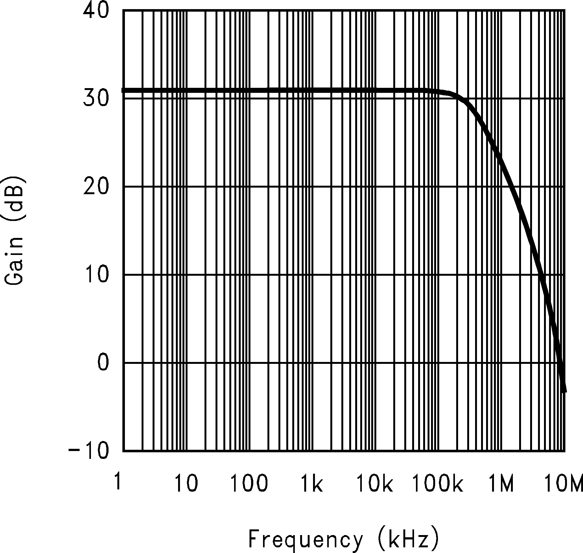 Figure 13. Error Amplifier Gain
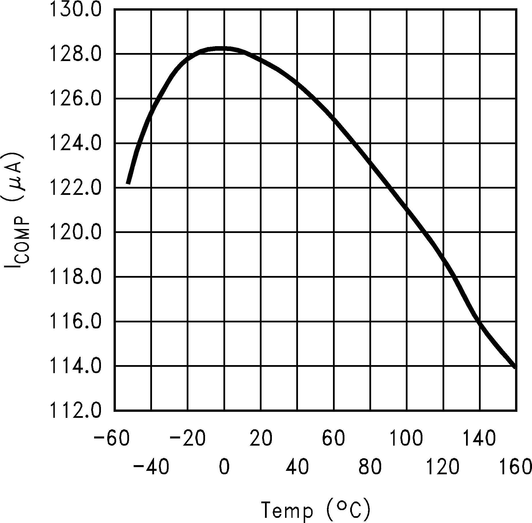 Figure 15. COMP Pin Source Current vs Temperature
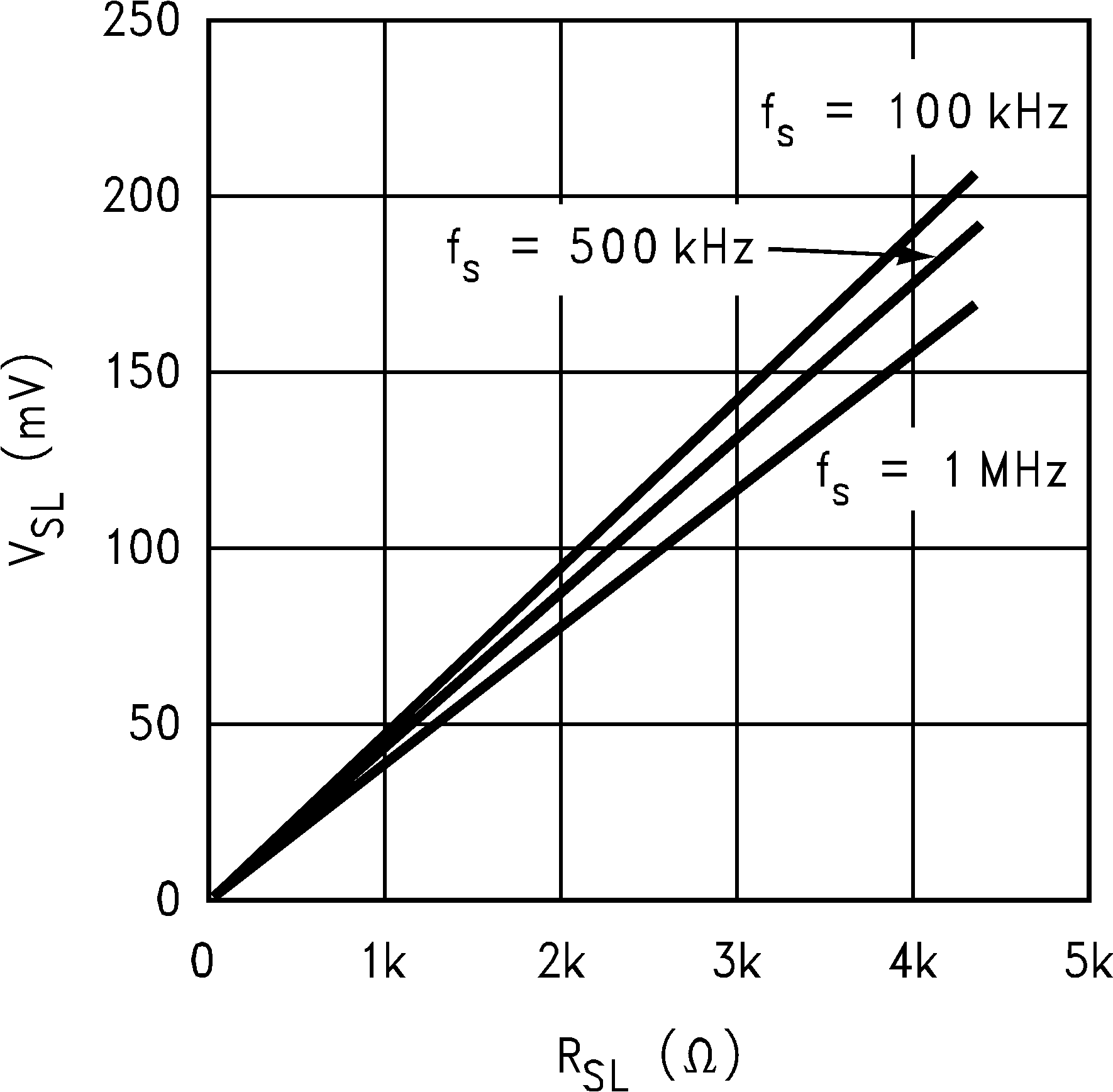 Figure 17. Compensation Ramp vs Compensation Resistor
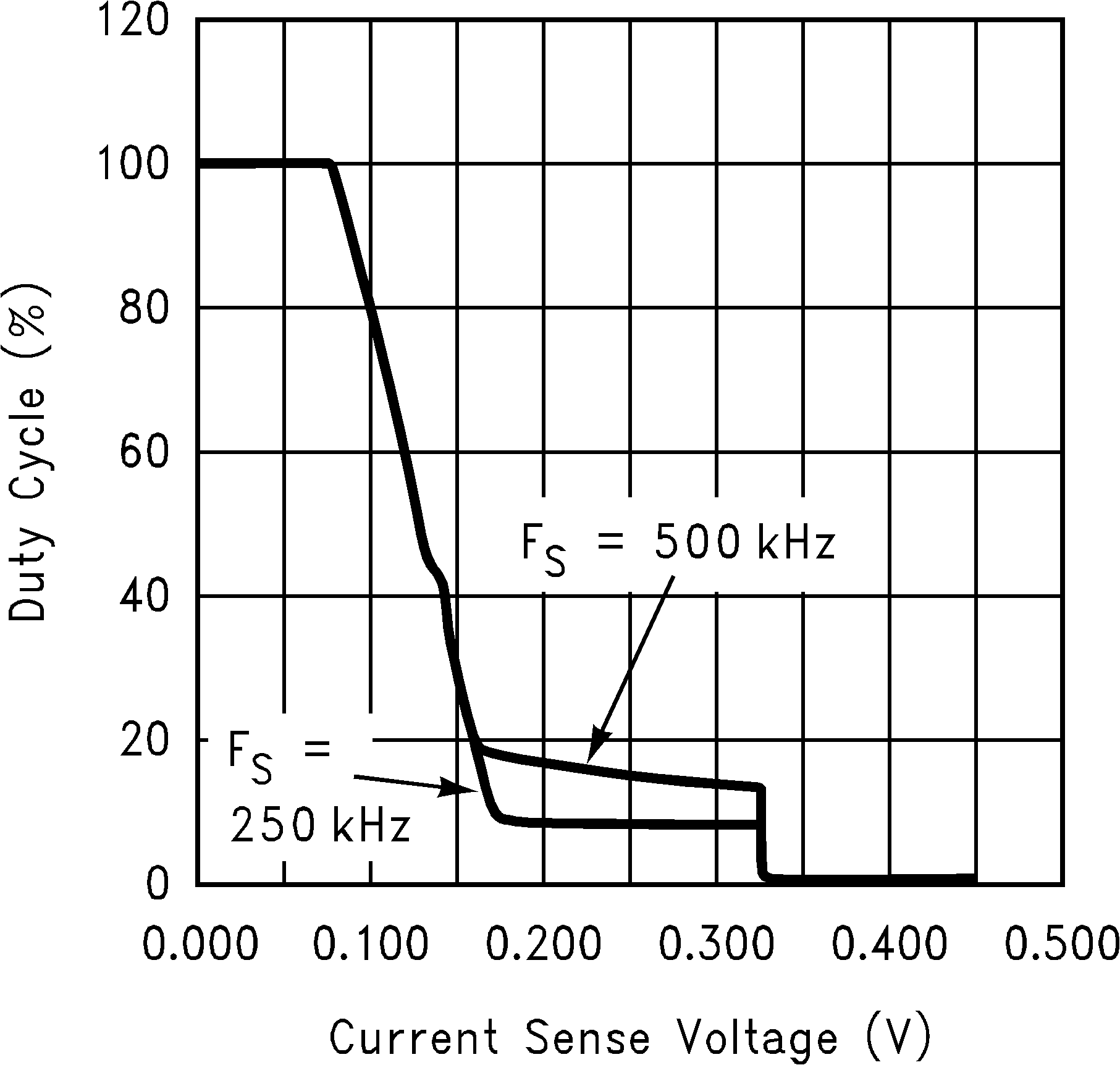 Figure 19. Current Sense Voltage vs Duty Cycle
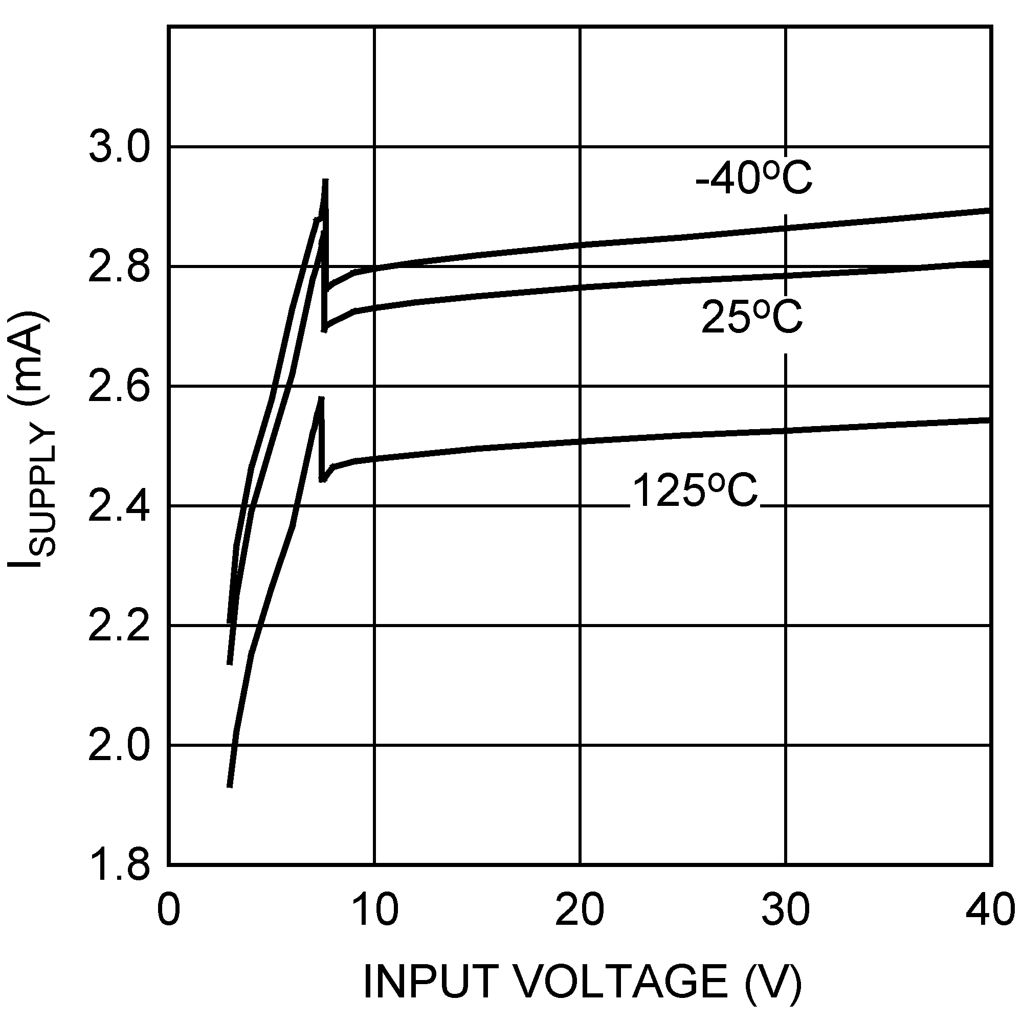 Figure 2. ISupply vs Input Voltage (Non-Switching)
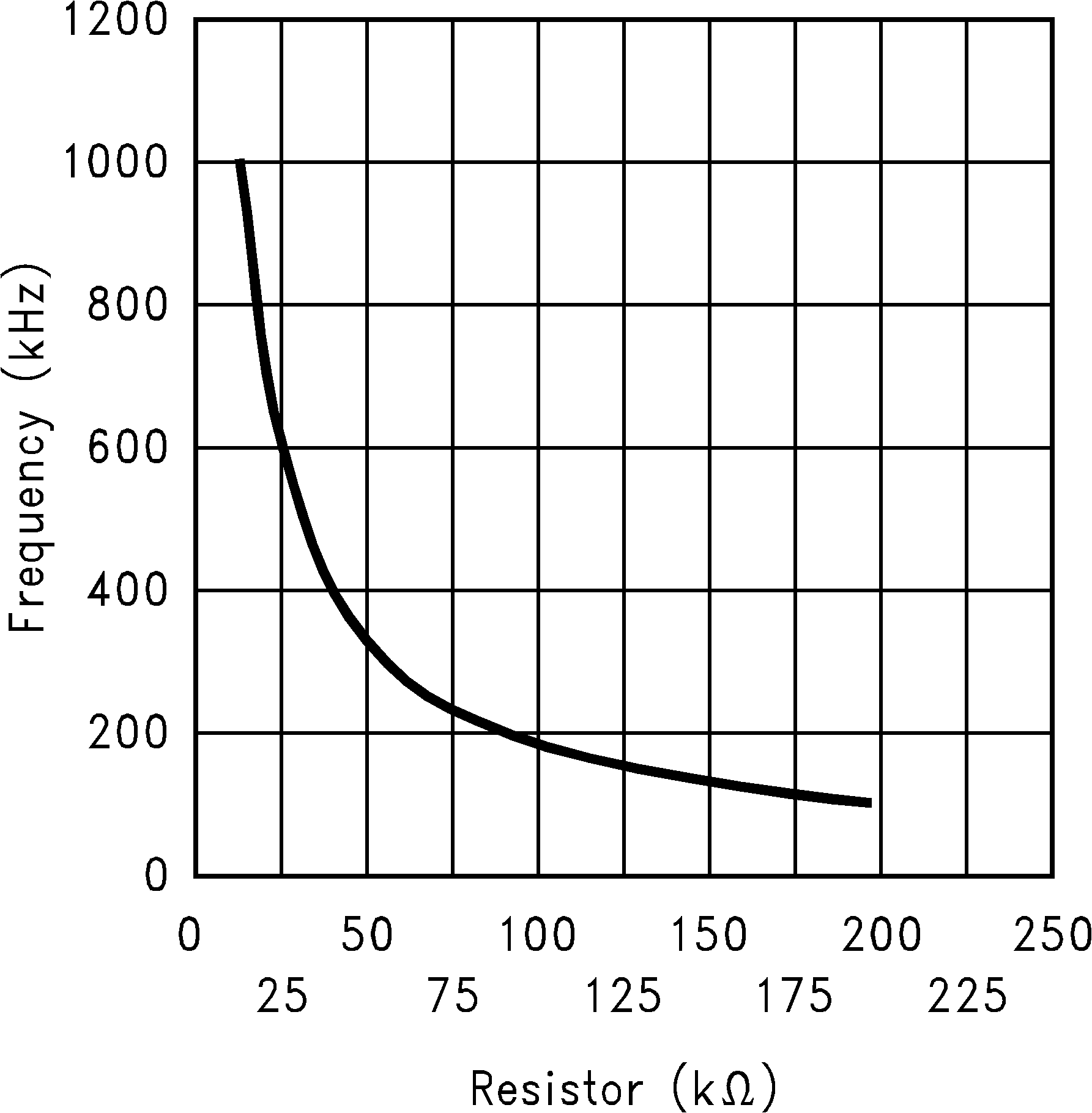 Figure 4. Switching Frequency vs RFA
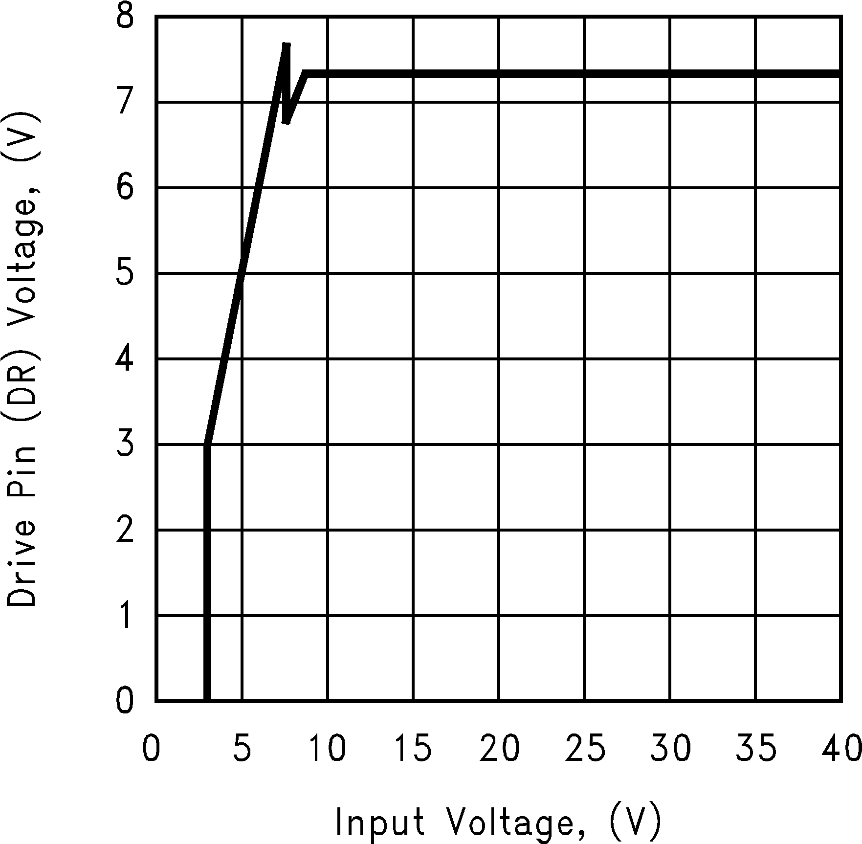 Figure 6. Drive Voltage vs Input Voltage
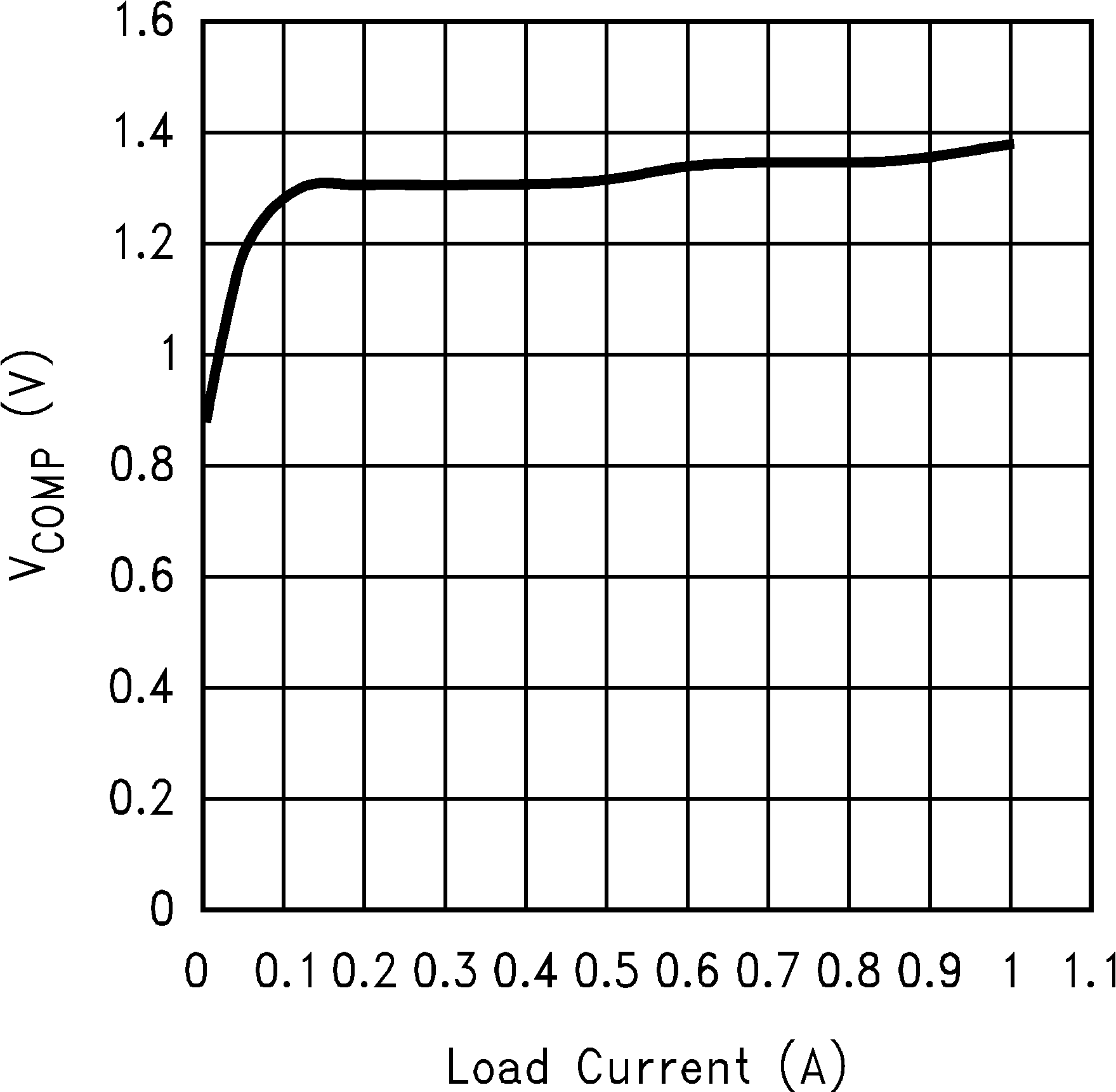 Figure 8. COMP Pin Voltage vs Load Current
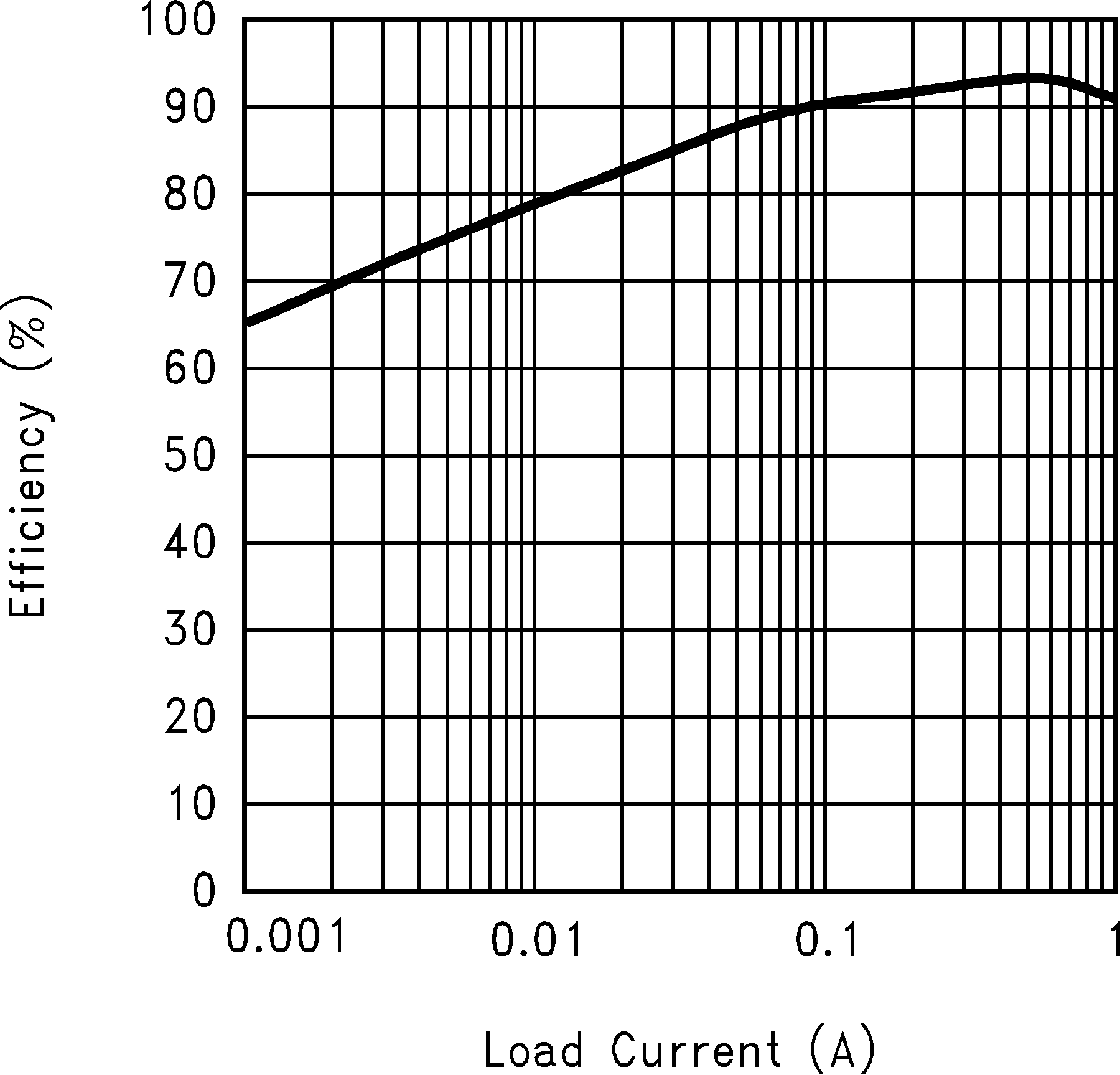 Figure 10. Efficiency vs Load Current (5 V In and 12 V Out)
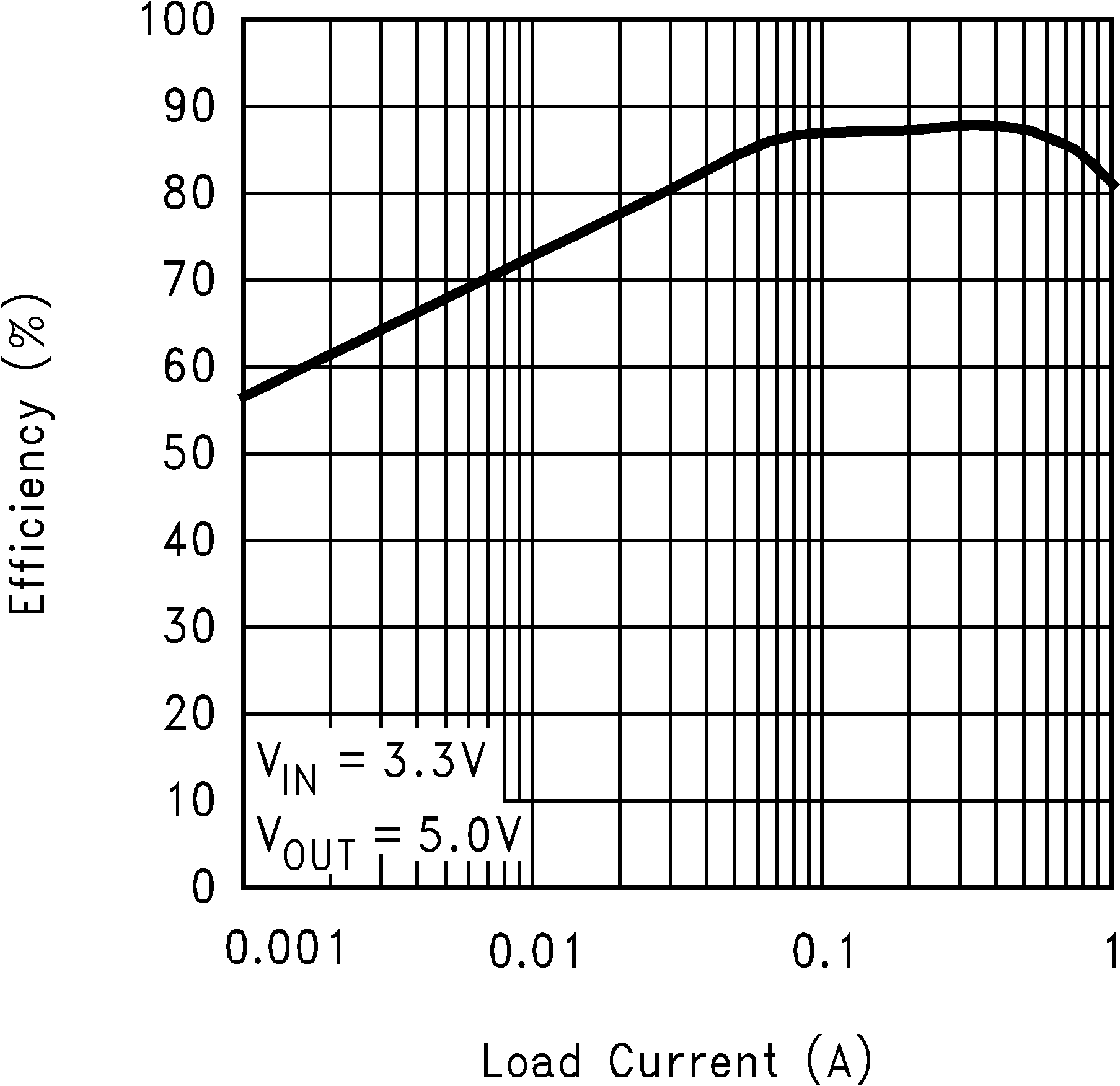 Figure 12. Efficiency vs Load Current (3.3 V In and 5 V Out)
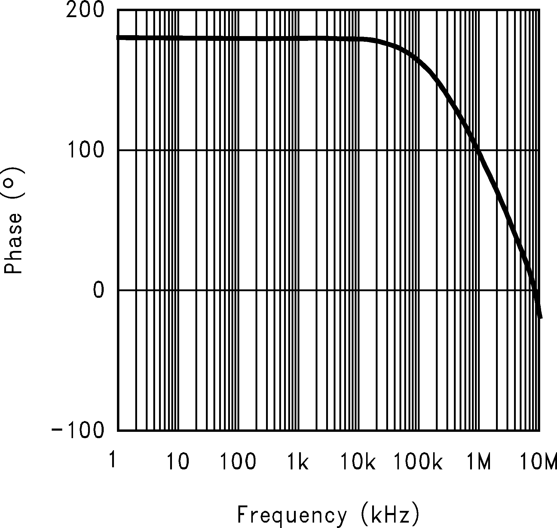 Figure 14. Error Amplifier Phase
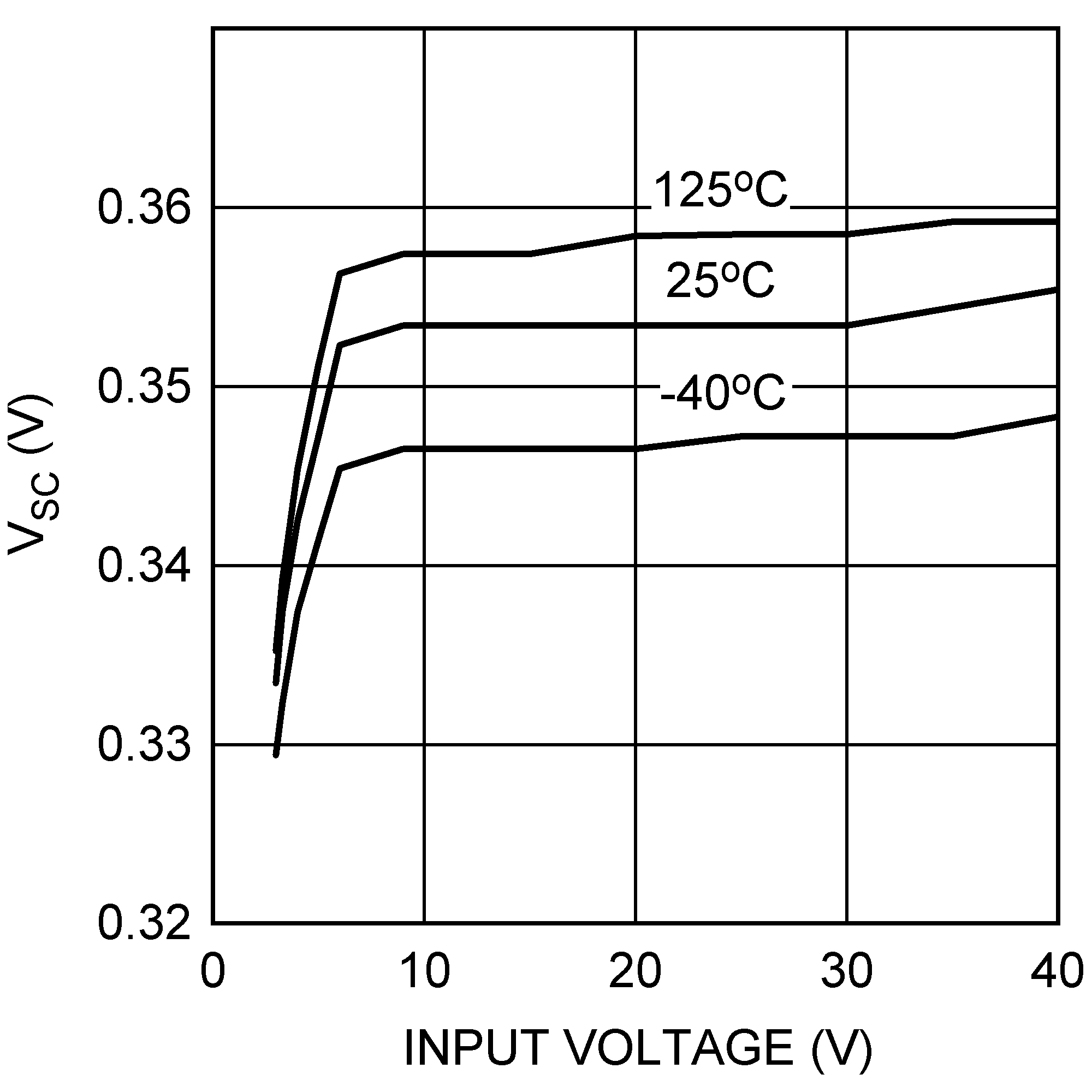 Figure 16. Short Circuit Protection vs Input Voltage
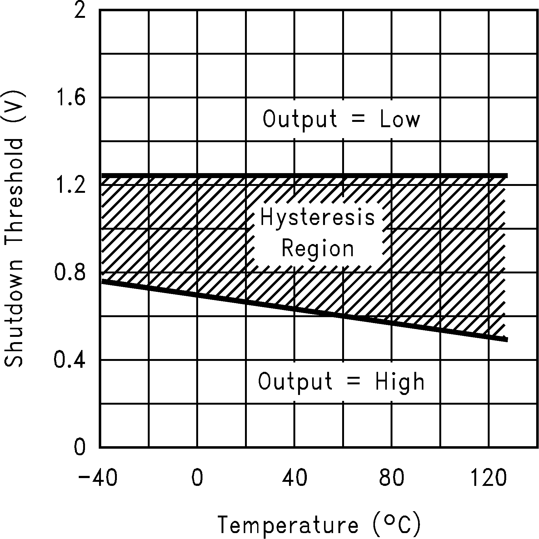 Figure 18. Shutdown Threshold Hysteresis vs Temperature