ZHCSK33G July 2008 – July 2019 LM3421 , LM3423
PRODUCTION DATA.
- 1 特性
- 2 应用
- 3 说明
- 4 修订历史记录
- 5 Device Comparison
- 6 Pin Configuration and Functions
- 7 Specifications
-
8 Detailed Description
- 8.1 Overview
- 8.2 Functional Block Diagram
- 8.3
Feature Description
- 8.3.1 Current Regulators
- 8.3.2 Predictive Off-Time (PRO) Control
- 8.3.3 Average LED Current
- 8.3.4 Analog Dimming
- 8.3.5 Current Sense and Current Limit
- 8.3.6 Overcurrent Protection
- 8.3.7 Zero Current Shutdown
- 8.3.8 Control Loop Compensation
- 8.3.9 Start-Up Regulator
- 8.3.10 Overvoltage Lockout (OVLO)
- 8.3.11 Input Undervoltage Lockout (UVLO)
- 8.3.12 PWM Dimming
- 8.3.13 LM3423 Only: DPOL, FLT, TIMR, and LRDY
-
9 Application and Implementation
- 9.1 Application Information
- 9.2
Typical Applications
- 9.2.1
Basic Topology Schematics
- 9.2.1.1 Design Requirements
- 9.2.1.2
Detailed Design Procedure
- 9.2.1.2.1 Operating Point
- 9.2.1.2.2 Switching Frequency
- 9.2.1.2.3 Average LED Current
- 9.2.1.2.4 Inductor Ripple Current
- 9.2.1.2.5 LED Ripple Current
- 9.2.1.2.6 Peak Current Limit
- 9.2.1.2.7 Loop Compensation
- 9.2.1.2.8 Input Capacitance
- 9.2.1.2.9 N-channel FET
- 9.2.1.2.10 Diode
- 9.2.1.2.11 Output OVLO
- 9.2.1.2.12 Input UVLO
- 9.2.1.2.13 PWM Dimming Method
- 9.2.1.2.14 Analog Dimming Method
- 9.2.2
LM3421 Buck-Boost Application
- 9.2.2.1 Design Requirements
- 9.2.2.2
Detailed Design Procedure
- 9.2.2.2.1 Operating Point
- 9.2.2.2.2 Switching Frequency
- 9.2.2.2.3 Average LED Current
- 9.2.2.2.4 Inductor Ripple Current
- 9.2.2.2.5 Output Capacitance
- 9.2.2.2.6 Peak Current Limit
- 9.2.2.2.7 Loop Compensation
- 9.2.2.2.8 Input Capacitance
- 9.2.2.2.9 N-channel FET
- 9.2.2.2.10 Diode
- 9.2.2.2.11 Input UVLO
- 9.2.2.2.12 Output OVLO
- 9.2.2.3 Application Curve
- 9.2.3 LM3421 BOOST Application
- 9.2.4 LM3421 Buck-Boost Application
- 9.2.5 LM3423 Boost Application
- 9.2.6 LM3421 Buck-Boost Application
- 9.2.7 LM3423 Buck Application
- 9.2.8 LM3423 Buck-Boost Application
- 9.2.9 LM3421 SEPIC Application
- 9.2.1
Basic Topology Schematics
- 10Power Supply Recommendations
- 11Layout
- 12器件和文档支持
- 13机械、封装和可订购信息
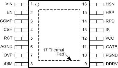
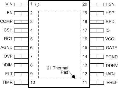
6 Pin Configuration and Functions
PWP Package
16-Pin HTSSOP
Top View

PWP Package
20-Pin HTSSOP
Top View

Pin Functions
| PIN | I/O(1) | FUNCTION | ||
|---|---|---|---|---|
| NAME | LM3423 | LM3421 | ||
| AGND | 6 | 6 | G | Analog ground. Connect to PGND through the DAP copper pad to provide ground return for CSH, COMP, RCT, and TIMR. |
| COMP | 3 | 3 | I | Compensation. Connect a capacitor to AGND to set the compensation. |
| CSH | 4 | 4 | I | Current sense high. Connect a resistor to AGND to set the signal current. For analog dimming, connect a controlled current source or a potentiometer to AGND as detailed in the Analog Dimming section. |
| DDRV | 13 | 9 | O | Dim gate drive output. Connect to the gate of the dimming MOSFET. |
| DPOL | 12 | — | I | Dim polarity. Connect to AGND if dimming with a series P-channel MOSFET or leave open when dimming with series N-channel MOSFET. |
| EN | 2 | 2 | I | Enable. Connect to AGND for zero current shutdown or apply more than 2.4 V to enable device. |
| FLT | 9 | — | I | Fault flag. Connect to pullup resistor from VIN and N-channel MOSFET open-drain output is high when a fault condition is latched by the timer. |
| GATE | 15 | 11 | O | Main gate drive output. Connect to the gate of the main switching MOSFET. |
| HSN | 20 | 16 | I | LED current sense negative. Connect through a series resistor to the negative side of the LED current sense resistor. |
| HSP | 19 | 15 | I | LED current sense positive. Connect through a series resistor to the positive side of the LED current sense resistor. |
| IS | 17 | 13 | I | Main switch current sense. Connect to the drain of the main N-channel MOSFET switch for RDS-ON sensing or to a sense resistor installed in the source of the same device. |
| LRDY | 11 | — | O | LED ready flag. Connect to pullup resistor from VIN and N-channel MOSFET open-drain output pulls down when the LED current is not in regulation. |
| nDIM | 8 | 8 | I | Dimming input and undervoltage protection. Connect a PWM signal for dimming as detailed in the PWM Dimming section and/or a resistor divider from VIN to program input undervoltage lockout (UVLO). Turnon threshold is 1.24 V and hysteresis for turnoff is provided by a 23-µA current source. |
| OVP | 7 | 7 | I | Overvoltage protection. Connect to a resistor divider from VO to program output overvoltage lockout (OVLO). Turnoff threshold is 1.24 V and hysteresis for turnon is provided by 23-µA current source. |
| PGND | 14 | 10 | G | Power ground. Connect to AGND through the DAP copper pad to provide ground return for GATE and DDRV. |
| RCT | 5 | 5 | I | Resistor capacitor timing. External RC network sets the predictive off-time and thus the switching frequency. |
| RPD | 18 | 14 | I | Resistor pulldown. Connect the low side of all external resistor dividers (VIN UVLO, OVP) to implement zero-current shutdown. |
| TIMR | 10 | — | I | Fault timer. Connect a capacitor to AGND to set the time delay before a sensed fault condition is latched. |
| VIN | 1 | 1 | I | Input voltage. Bypass with 100-nF capacitor to AGND as close to the device as possible in the printed-circuit-board layout. |
| VCC | 16 | 12 | I | Internal regulator output. Bypass with 2.2-µF to 3.3-µF ceramic capacitor to PGND. |
| Thermal PAD | G | Thermal PAD on bottom of IC. Star ground, connecting AGND and PGND. | ||
| DAP | DAP (21) | DAP (17) | G | Star ground, connecting AGND and PGND. |
(1) G = Ground, I = Input, O = Output