SNVS116E May 1998 – December 2014 LM3420
PRODUCTION DATA.
- 1 Features
- 2 Applications
- 3 Description
- 4 Revision History
- 5 Pin Configuration and Functions
- 6 Specifications
- 7 Parameter Measurement Information
- 8 Detailed Description
-
9 Application and Implementation
- 9.1 Application Information
- 9.2
Typical Application: Constant Current/Constant Voltage Li-Ion Battery Charger
- 9.2.1 Design Requirements
- 9.2.2 Detailed Design Procedure
- 9.2.3 Application Curve
- 9.2.4
Other Application Circuits
- 9.2.4.1 Low Dropout Constant Current/Constant Voltage 2-Cell Charger
- 9.2.4.2 High-Efficiency Switching Regulator Constant Current/Constant Voltage 2-Cell Charger
- 9.2.4.3 Low Dropout Constant Current/Constant Voltage Li-Ion Battery Charger
- 9.2.4.4 High-Efficiency Switching Charger With High Side Current Sensing
- 9.2.4.5 Fast-Pulsed Constant Current 2-Cell Charger
- 9.2.4.6 MOSFET Low Dropout Charger
- 10Power Supply Recommendations
- 11Layout
- 12Device and Documentation Support
- 13Mechanical, Packaging, and Orderable Information
5 Pin Configuration and Functions
SOT-23 (DBV) Package
5 Pins
Top
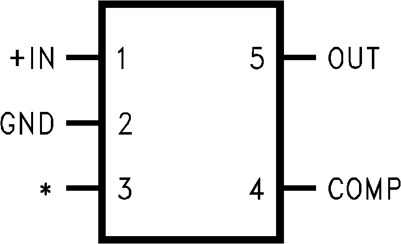
Pin Functions
| PIN | I/O | DESCRIPTION | |
|---|---|---|---|
| NAME | NUMBER | ||
| IN | 1 | I | Input voltage supply |
| GND | 2 | — | Ground |
| NC | 3 | — | No connection |
| OUT | 4 | O | Open emitter output capable of sourcing current |
| COMP | 5 | Compensation | |