SNVS113F December 1999 – May 2016 LM3411
PRODUCTION DATA.
- 1 Features
- 2 Applications
- 3 Description
- 4 Revision History
- 5 Pin Configuration and Functions
- 6 Specifications
- 7 Parameter Measurement Information
- 8 Detailed Description
-
9 Application and Implementation
- 9.1 Application Information
- 9.2
Typical Applications
- 9.2.1 LM3411 Typical Application
- 9.2.2 Isolated 250-mA Flyback Switching Regulator
- 9.2.3 Isolated 1.5-A Flyback Switching Regulator
- 9.2.4 Precision 1-A Buck Regulator
- 9.2.5 Negative Input, Negative or Positive Output Flyback Regulator
- 9.2.6 Precision 5-V, 1-A Low Dropout Regulator
- 9.2.7 3.3-V, 0.5-A Low Dropout Regulator
- 9.2.8 Precision Positive Voltage Regulator With Accurate Current Limit
- 9.2.9 Precision Negative Voltage Regulator
- 9.2.10 4.7-V Power ON Detector With Hysteresis
- 9.2.11 ±50-mV External Trim
- 9.2.12 250-mA Shunt Regulator
- 9.2.13 Voltage Detector
- 9.2.14 Overvoltage Crowbar
- 10Power Supply Recommendations
- 11Layout
- 12Device and Documentation Support
- 13Mechanical, Packaging, and Orderable Information
9 Application and Implementation
NOTE
Information in the following applications sections is not part of the TI component specification, and TI does not warrant its accuracy or completeness. TI’s customers are responsible for determining suitability of components for their purposes. Customers should validate and test their design implementation to confirm system functionality.
9.1 Application Information
The LM3411 is a high-efficiency shunt regulator optimized for driving an opto-coupler in an isolated feedback system. This enables accurate regulation of the output voltage as well as convenient drive to the opto-coupler in a small SOT-23 package. In addition to isolated feedback systems the LM3411 is also applicable to a wide variety of linear regulator applications.
9.2 Typical Applications
9.2.1 LM3411 Typical Application
Figure 19 shows a typical use case for the LM3411. Here, the device is used as a precision shunt regulator to control the output voltage of a switching power supply. The LM3411 provides the functionality necessary to drive the external opto-coupler, an on-board reference necessary for precision control of the DC output voltage, and an on-board operational amplifier for providing the necessary compensation to optimize the transient performance of the system.
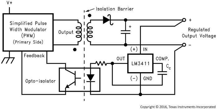 Figure 19. LM3411 Typical Application Schematic
9.2.1.1 Design Requirements
The following sections provide a variety of application level design examples. See the following for the basic requirements.
● Isolated flyback converter example is 5 V with 250 mA.
● Isolated flyback converter example is 3.3 V or 5 V with 1.5 A.
● Buck converter example is 5 V with 1 A.
● Flyback converter example is VIN = –20 V to –10 V and VOUT = –5 V with 1 A.
● Low dropout linear regulator example is 5 V with 1 A.
● Low dropout linear regulator example is 3.3 V and 0.5 A.
● Precision positive voltage regulator with accurate current limit is VIN = 9 V to 20 V and VOUT = 5 V.
● Negative voltage regulator example is VIN = –8 V to –20 V and VOUT = –5 V.
● 250-mA shunt regulator example is VOUT = 5 V.
9.2.1.2 Detailed Design Procedure
9.2.1.2.1 Compensation
The inverting input of the error amplifier is brought out to allow overall closed-loop compensation. In many of the applications circuits shown in the subsequent sections, compensation is provided by a single capacitor connected from the compensation pin to the out pin of the LM3411. The capacitor values shown in the schematics accompanying these sections are adequate under most conditions, but they can be increased or decreased depending on the desired loop response. Applying a load pulse to the output of a regulator circuit and observing the resultant output voltage response is a easy method of determining the stability of the control loop. Analyzing more complex feedback loops requires additional information.
The formula for AC gain at a frequency (f) as in Equation 1.
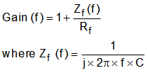
where
- Rf ≈ 52 kΩ for the 3.3-V part
- Rf ≈ 94 kΩ for the 5-V part
The resistor (Rf) in the formula is an internal resistor located on the die. Since this resistor value will affect the phase margin, the worst case maximum and minimum values are important when analyzing closed loop stability. The minimum and maximum room temperature values of this resistor are specified in Electrical Characteristics: 3.3-V Version of this data sheet, and Figure 11 shows the temperature coefficient from Typical Characteristics. In the applications shown in the subsequent sections, the worst case phase margin occurs with minimum values of Rf.
9.2.1.2.2 Test Circuit
The test circuit shown in Figure 20 can be used to measure and verify various LM3411 parameters. Test conditions are set by forcing the appropriate voltage at the VOUT Set test point and selecting the appropriate RL or IOUT as specified in Electrical Characteristics. Use a DVM at the measure test points to read the data.
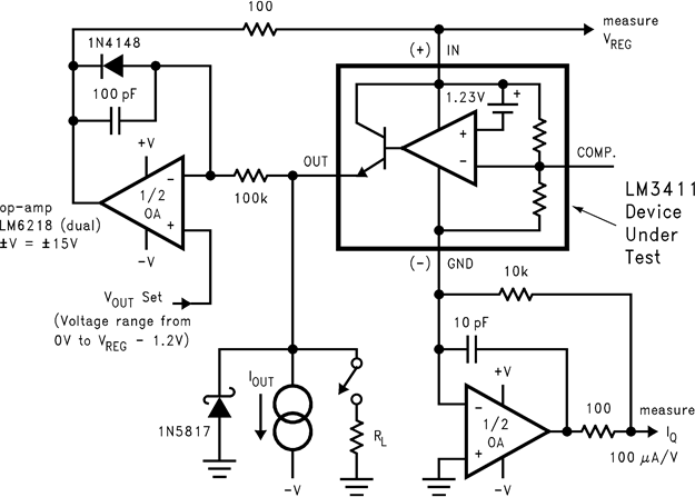 Figure 20. LM3411 Test Circuit
9.2.1.3 Application Curves
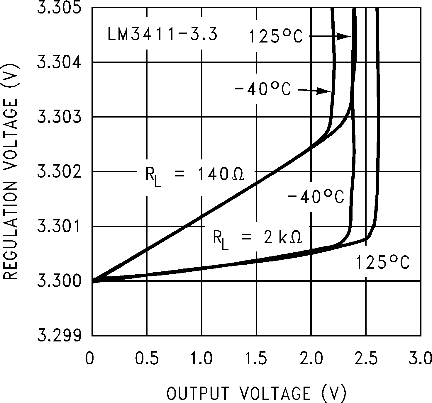 Figure 21. Regulation Voltage vs Output Voltage
and Load Resistance
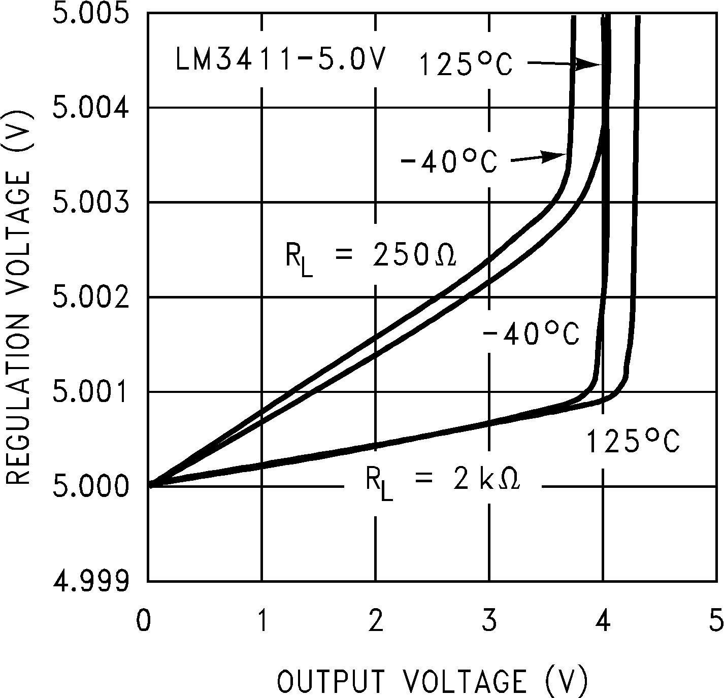 Figure 22. Regulation Voltage vs Output Voltage
and Load Resistance
9.2.2 Isolated 250-mA Flyback Switching Regulator
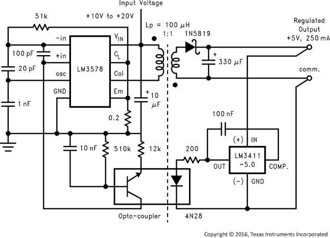 Figure 23. Isolated 250-mA Flyback Switching Regulator Schematic
9.2.2.1 Design Requirements
The design requirements for this isolated flyback converter example are 5 V with 250 mA.
9.2.2.2 Detailed Design Procedure
The LM3411 regulator or driver provides the reference and feedback drive functions in a regulated power supply. It can also be used together with many different types of regulators, (both linear and switching) as well as other power semiconductor devices to add precision and improve regulation specifications. Output voltage tolerances better than 0.5% are possible without using trim pots or precision resistors.
One of the main applications of the LM3411 is to drive an opto-isolator to provide feedback signal isolation in a switching regulator circuit. For low current applications (up to 250 mA), see Figure 23 for a circuit that provides good regulation and complete input and output electrical isolation.
For an input voltage of 15 V, this circuit can provide an output of either 3.3 V or 5 V with a load current up to
250 mA with excellent regulation characteristics. With the part values shown, this circuit operates at 80 kHz, and can be synchronized to a clock or an additional LM3578. See LM3578A's data sheet (SNVS767) for additional information.
9.2.3 Isolated 1.5-A Flyback Switching Regulator
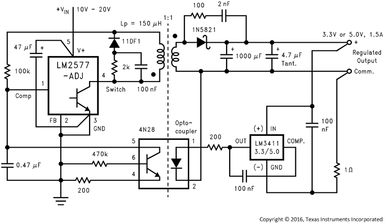 Figure 24. Isolated 1.5-A Flyback Switching Regulator Using a LM2577
9.2.3.1 Design Requirements
The design requirements for this isolated flyback converter example are 3.3 V or 5 V with 1.5 A.
9.2.3.2 Detailed Design Procedure
An isolated DC-DC flyback converter capable of higher output current is shown in Figure 24. This circuit uses the LM2577 SIMPLE SWITCHER voltage regulator for the Pulse Width Modulation (PWM), power switch, and protection functions, while the LM3411 provides the voltage reference, gain, and opto-coupler drive functions. In this circuit, the reference and error amplifier in the LM2577 are not used (note that the feedback pin is grounded). The gain is provided by the LM3411. Since the voltage reference is located on the secondary side of the transformer, this circuit provides very good regulation specifications.
The output of a switching regulator typically will contain a small ripple voltage at the switching frequency and may also contain voltage transients. These transient voltage spikes can be sensed by the LM3411 and could give an incorrect regulation voltage. An RC filter consisting of a 1-Ω resistor and a 100-nF capacitor will filter these transients and minimize this problem. The 1-Ω resistor should be located on the ground side of the LM3411, and the capacitor should be physically located near the package.
9.2.4 Precision 1-A Buck Regulator
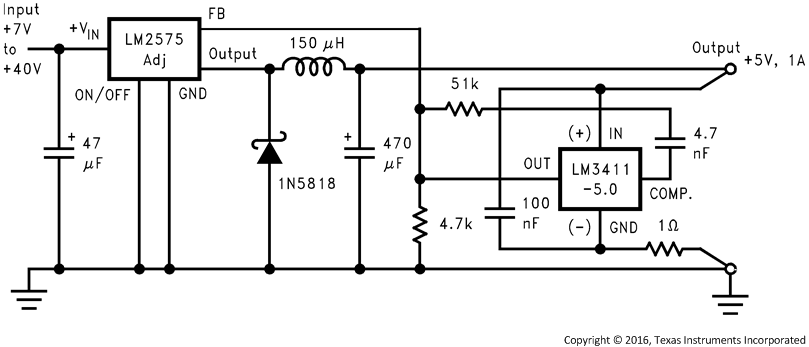 Figure 25. Precision 1-A Buck Regulator Schematic
9.2.4.1 Design Requirements
The design requirements for this precision buck converter example are 5 V with 1 A.
9.2.4.2 Detailed Design Procedure
Improved output voltage tolerance and regulation specifications are possible by combining the LM3411A with one of the SIMPLE SWITCHER buck regulator IC's, such as the LM2574, LM2575, or LM2576. Figure 25 shows a circuit capable of providing a 5-V, ±0.5% output (1% over the operating temperature range) without using any trim-pots or precision resistors. Typical line regulation numbers are a 1 mV change on the output for a 8 V to
18 V change on the input, and load regulation of 1 mV with a load change from 100 mA to 1 A.
9.2.5 Negative Input, Negative or Positive Output Flyback Regulator
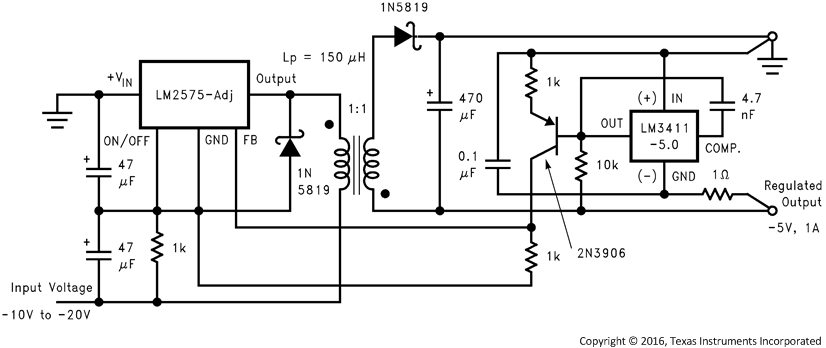 Figure 26. Negative Input, Negative or Positive Output Flyback Regulator Schematic
9.2.5.1 Design Requirements
The design requirements for this flyback converter example are VIN = –20 V to –10 V and VOUT = –5 V with 1 A.
9.2.5.2 Detailed Design Procedure
A DC-DC flyback converter that accepts a negative input voltage, and delivers either a positive or negative output is shown in Figure 26. The circuit uses a buck regulator (such as the LM2574, LM2575, or LM2576, depending on how much output current is needed) operating in a flyback configuration. The LM3411 provides the reference and the required level shifting circuitry needed to make the circuit work correctly.
A unique feature of this circuit is the ability to ground either the high or low side of the output, thus generating either a negative or a positive output voltage. Although no isolation is provided, with the addition of an opto-isolator and related components, this circuit could provide input/output isolation.
Combining a LM3411A 5-V version with a 1-A low dropout linear regulator results in a 5 V ±0.5% (1% over the operating temperature range) regulator with excellent regulation specifications, with no trimming or 1% resistors needed.
An added benefit of this circuit (and also true of many of the other circuits shown) is the high-side and low-side remote output voltage sensing feature. Sensing the output voltage at the load eliminates the voltage drops associated with wire resistance, thus providing near perfect load regulation.
9.2.6 Precision 5-V, 1-A Low Dropout Regulator
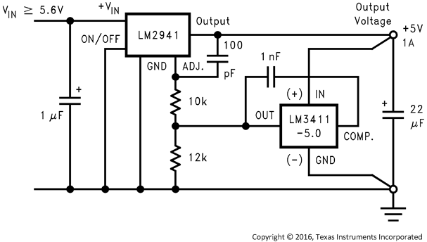 Figure 27. Precision 5-V, 1-A Low Dropout Regulator
9.2.6.1 Design Requirements
The design requirements for this precision low dropout linear regulator example are 5 V with 1 A.
9.2.6.2 Detailed Design Procedure
Figure 27 shows a 5-V, 1-A regulator circuit featuring low dropout, very good regulation specifications, self-protection features, and allows output voltage sensing. The regulator used is a LM2941 adjustable low dropout positive regulator, which also features an ON/OFF pin to provide a shutdown feature.
9.2.7 3.3-V, 0.5-A Low Dropout Regulator
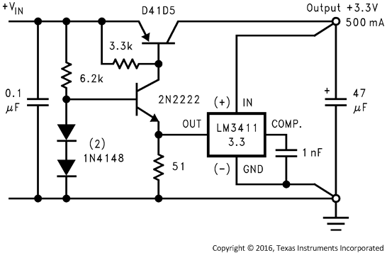 Figure 28. 3.3-V, 0.5-A Low Dropout Regulator Schematic
9.2.7.1 Design Requirements
The design requirements for this low dropout linear regulator example are 3.3 V and 0.5 A.
9.2.7.2 Detailed Design Procedure
The circuit in Figure 28 shows a 3.3-V low dropout regulator using the LM3411-3.3 and several discrete components. This circuit is capable of excellent performance with both the dropout voltage and the ground pin current specifications improved over the LM2941 and LM3411 circuit.
9.2.8 Precision Positive Voltage Regulator With Accurate Current Limit
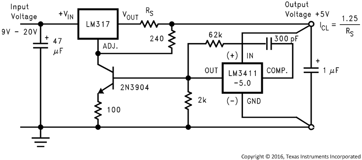 Figure 29. Precision Positive Voltage Regulator With Accurate Current Limit Schematic
9.2.8.1 Design Requirements
The design requirements for this precision positive voltage regulator with accurate current limit are VIN = 9 V to 20 V and VOUT = 5 V.
9.2.8.2 Detailed Design Procedure
The standard LM317 three terminal adjustable regulator circuit can greatly benefit by adding a LM3411. Performance is increased and features are added. Figure 29 shows a circuit capable of providing further improved line and load regulation, lower temperature drift, and full remote output voltage sensing on both the high and low side. In addition, a precise current limit or constant current feature is simple to add.
Current limit protection in most IC regulators is mainly to protect the IC from gross overcurrent conditions which could otherwise fuse bonding wires or blow IC metalization, therefore not much precision is needed for the actual current limit values. Current limit tolerances can sometimes vary from ±10% to as high as +300% over manufacturing and temperature variations. Often critical circuitry requires a much tighter control over the amount of current the power supply can deliver. For example, a power supply may be needed that can deliver 100% of its design current, but can still limit the maximum current to 110% to protect critical circuitry from high current fault conditions.
The circuit in Figure 29 can provide a current limit accuracy that is better than ±4%, over all possible variations, in addition to having excellent line, load, and temperature specifications.
9.2.9 Precision Negative Voltage Regulator
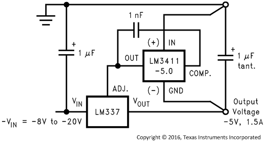 Figure 30. Precision Negative Voltage Regulator Schematic
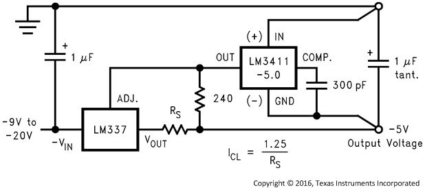 Figure 31. Precision Negative Voltage Regulator With Accurate Current Limit
9.2.9.1 Design Requirements
The design requirements for this negative voltage regulator example are VIN = –8 V to –20 V and VOUT = –5 V.
9.2.9.2 Detailed Design Procedure
Like the positive regulators, the performance of negative adjustable regulators can also be improved by adding the LM3411. Output voltages of either 3.3 V or 5 V at currents up to 1.5 A (3 A when using a LM333) are possible. Adding two resistors to the circuit in Figure 30 adds the precision current limit feature as shown in Figure 31. Current limit tolerances of ±4% over manufacturing and temperature variations are possible with this circuit.
9.2.10 4.7-V Power ON Detector With Hysteresis
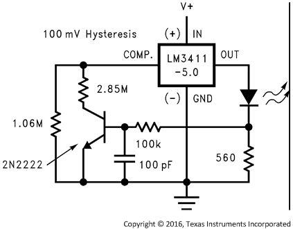 Figure 32. 4.7-V Power ON Detector With Hysteresis Schematic
9.2.10.1 Detailed Design Procedure
Figure 32 shows a simple 5-V supply monitor circuit. Using the LM3411's voltage reference, operational amplifier (as a comparator) and output driver, this circuit provides a LED indication of the presence of the 5-V supply.
9.2.11 ±50-mV External Trim
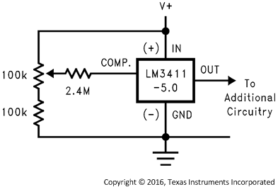 Figure 33. ±50-mV External Trim Schematic
9.2.11.1 Detailed Design Procedure
The LM3411 initial room temperature tolerance is ±1% and ±0.5% for the A grade part. If a tighter tolerance is needed, see Figure 33 for a trim scheme that provides approximately ±1% adjustment range of the regulation voltage (VREG).
9.2.12 250-mA Shunt Regulator
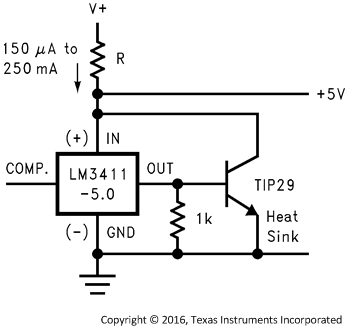 Figure 34. 250-mA Shunt Regulator Schematic
9.2.12.1 Design Requirements
The design requirement for this 250-mA shunt regulator example is VOUT = 5 V.
9.2.12.2 Detailed Design Procedure
The LM3411 is ensured to drive a 15 mA load, but if more current is needed, a NPN boost transistor can be added. Figure 34 shows a shunt regulator capable of providing excellent regulation over a very wide range of current.
9.2.13 Voltage Detector
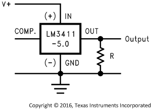 Figure 35. Voltage Detector Schematic
9.2.13.1 Detailed Design Procedure
Perhaps one of the simplest applications for the LM3411 is the voltage detector circuit shown in Figure 35. The OUT pin is low when the input voltage is less than VREG. When the VIN pin rises above VREG, the OUT pin is pulled high by the internal NPN output resistor.
9.2.14 Overvoltage Crowbar
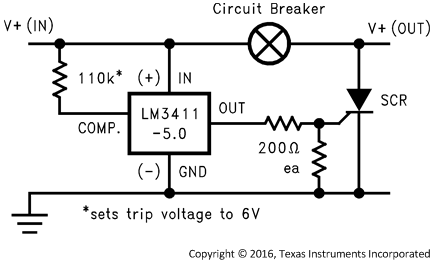 Figure 36. Overvoltage Crowbar Schematic
9.2.14.1 Detailed Design Procedure
Also an overvoltage detector, the crowbar circuit shown in Figure 36 is normally located at the output of a power supply to protect the load from an overvoltage condition should the power supply fail with an input/output short.