SLVS047L November 1981 – January 2015 LM237 , LM337
PRODUCTION DATA.
- 1 Features
- 2 Applications
- 3 Description
- 4 Simplified Schematic
- 5 Revision History
- 6 Pin Configuration and Functions
- 7 Specifications
- 8 Detailed Description
- 9 Application and Implementation
- 10Power Supply Recommendations
- 11Layout
- 12Device and Documentation Support
- 13Mechanical, Packaging, and Orderable Information
封装选项
机械数据 (封装 | 引脚)
散热焊盘机械数据 (封装 | 引脚)
订购信息
8 Detailed Description
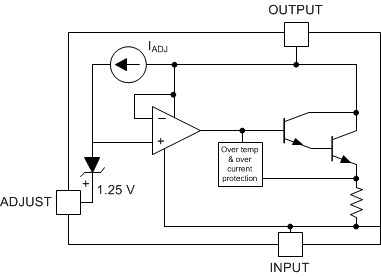
8.1 Overview
The LMx37 devices are adjustable 3-terminal negative-voltage regulators capable of supplying in excess of –1.5 A over an output voltage range of –1.2 V to –37 V. They are exceptionally easy to use, requiring only two external resistors to set the output voltage and one output capacitor for frequency compensation. The current design is optimized for excellent regulation and low thermal transients. In addition, LM237 and LM337 feature internal current limiting, thermal shutdown, and safe-area compensation, making them virtually immune to failure by overloads. The LMx37 devices serve a wide variety of applications, including local on-card regulation, programmable output-voltage regulation, and precision current regulation.
8.2 Functional Block Diagram
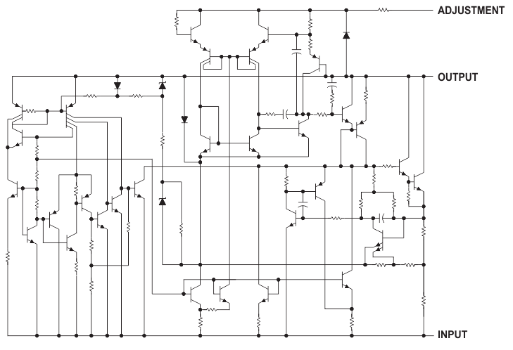
8.3 Design Schematic
8.4 Feature Description
8.4.1 Output Voltage Adjustment
The ADJUSTMENT pin serves as a voltage adjustment reference for the output. The ADJUSTMENT pin can be attached to a resistor divider circuit to adjust its own voltage level. The reference voltage VADJUSTMENT will typically be 1.25 V higher than VO.
8.5 Device Functional Modes
8.5.1 Adjustable Output Mode
The device has a single functional mode: Adjustable output voltage mode. A resistor divider circuit on the ADJUSTMENT pin determines the output voltage.