SNVS778E May 1999 – January 2016 LM137 , LM337-N
PRODUCTION DATA.
- 1 Features
- 2 Applications
- 3 Description
- 4 Revision History
- 5 Pin Configuration and Functions
- 6 Specifications
- 7 Detailed Description
- 8 Application and Implementation
- 9 Power Supply Recommendations
- 10Layout
- 11Device and Documentation Support
- 12Mechanical, Packaging, and Orderable Information
封装选项
机械数据 (封装 | 引脚)
散热焊盘机械数据 (封装 | 引脚)
- DCY|4
订购信息
6 Specifications
6.1 Absolute Maximum Ratings
6.2 ESD Ratings
| VALUE | UNIT | |||
|---|---|---|---|---|
| V(ESD) | Electrostatic discharge | Human-body model (HBM), per ANSI/ESDA/JEDEC JS-001(1) | ±2000 | V |
(1) JEDEC document JEP155 states that 500-V HBM allows safe manufacturing with a standard ESD control process. Pins listed as ±2000 V may actually have higher performance.
6.3 Recommended Operating Conditions
over operating free-air temperature range (unless otherwise noted)| MIN | MAX | UNIT | |||
|---|---|---|---|---|---|
| Operating junction temperature | LM137 | –55 | 150 | °C | |
| LM337-N | 0 | 125 | |||
| LM337I | –40 | 125 | |||
6.4 Thermal Information
| THERMAL METRIC(1) | LM137 | LM337-N | UNIT | |||
|---|---|---|---|---|---|---|
| NDT (TO) |
NDT (TO) |
DCY (SOT-223) |
NDE OR NDG (TO-220) |
|||
| 3 PINS | 3 PINS | 3 PINS | 3 PINS | |||
| RθJA | Junction-to-ambient thermal resistance | 140(2) | 140(2) | 58.3 | 22.9 | °C/W |
| RθJC(top) | Junction-to-case (top) thermal resistance | 12 | 12 | 36.6 | 15.7 | °C/W |
| RθJB | Junction-to-board thermal resistance | — | — | 7.2 | 4.1 | °C/W |
| ψJT | Junction-to-top characterization parameter | — | — | 1.3 | 2.4 | °C/W |
| ψJB | Junction-to-board characterization parameter | — | — | 7 | 4.1 | °C/W |
| RθJC(bot) | Junction-to-case (bottom) thermal resistance | — | — | — | 1 | °C/W |
(1) For more information about traditional and new thermal metrics, see the Semiconductor and IC Package Thermal Metrics application report, SPRA953.
(2) No heat sink.
6.5 Electrical Characteristics
Unless otherwise specified, these specifications apply −55°C ≤ Tj ≤ 150°C for the LM137, 0°C ≤ Tj ≤ 125°C for the LM337-N; VIN − VOUT = 5 V; and IOUT = 0.1 A for the TO package and IOUT = 0.5 A for the SOT-223 and TO-220 packages. Although power dissipation is internally limited, these specifications are applicable for power dissipations of 2 W for the TO and SOT-223, and 20 W for the TO-220. IMAX is 1.5 A for the SOT-223 and TO-220 packages, and 0.2 A for the TO package.| PARAMETER | TEST CONDITIONS | LM137 | LM337-N | UNIT | |||||
|---|---|---|---|---|---|---|---|---|---|
| MIN | TYP | MAX | MIN | TYP | MAX | ||||
| Line regulation | TJ = 25°C, 3 V ≤ |VIN − VOUT| ≤ 40 V(1)
IL = 10 mA |
0.01 | 0.02 | 0.01 | 0.04 | %/V | |||
| Load regulation | TJ = 25°C, 10 mA ≤ IOUT ≤ IMAX | 0.3% | 0.5% | 0.3% | 1% | ||||
| Thermal regulation | TJ = 25°C, 10-ms Pulse | 0.002 | 0.02 | 0.003 | 0.04 | %/W | |||
| Adjustment pin current | 65 | 100 | 65 | 100 | μA | ||||
| Adjustment pin current charge | 10 mA ≤ IL ≤ IMAX
3 V ≤ |VIN − VOUT| ≤ 40 V, TA = 25°C |
2 | 5 | 2 | 5 | μA | |||
| Reference voltage | 3 V ≤ |VIN − VOUT| ≤ 40 V, (2)
10 mA ≤ IOUT ≤ IMAX, P ≤ PMAX |
TJ = 25°C (2) | −1.225 | −1.25 | −1.275 | −1.213 | −1.25 | −1.287 | V |
| −55°C ≤ TJ ≤ 150°C | −1.2 | −1.25 | −1.3 | −1.2 | −1.25 | −1.3 | V | ||
| Line regulation | 3 V ≤ |VIN − VOUT| ≤ 40 V, (1) | 0.02 | 0.05 | 0.02 | 0.07 | %/V | |||
| Load regulation | 10 mA ≤ IOUT ≤ IMAX, (1) | 0.3% | 1% | 0.3% | 1.5% | ||||
| Temperature stability | TMIN ≤ Tj ≤ TMAX | 0.6% | 0.6% | ||||||
| Minimum load current | |VIN − VOUT| ≤ 40 V | 2.5 | 5 | 2.5 | 10 | mA | |||
| |VIN − VOUT| ≤ 10 V | 1.2 | 3 | 1.5 | 6 | mA | ||||
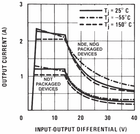
| Current limit | |VIN − VOUT| ≤ 15 V | K, DCY and NDE package | 1.5 | 2.2 | 3.5 | 1.5 | 2.2 | 3.7 | A |
| NDT package | 0.5 | 0.8 | 1.8 | 0.5 | 0.8 | 1.9 | A | ||
| |VIN − VOUT| = 40 V, TJ = 25°C | K, DCY and NDE package | 0.24 | 0.4 | 0.15 | 0.4 | A | |||
| NDT package | 0.15 | 0.17 | 0.1 | 0.17 | A | ||||
| RMS output noise, % of VOUT | Tj = 25°C, 10 Hz ≤ f ≤ 10 kHz | 0.003% | 0.003% | ||||||
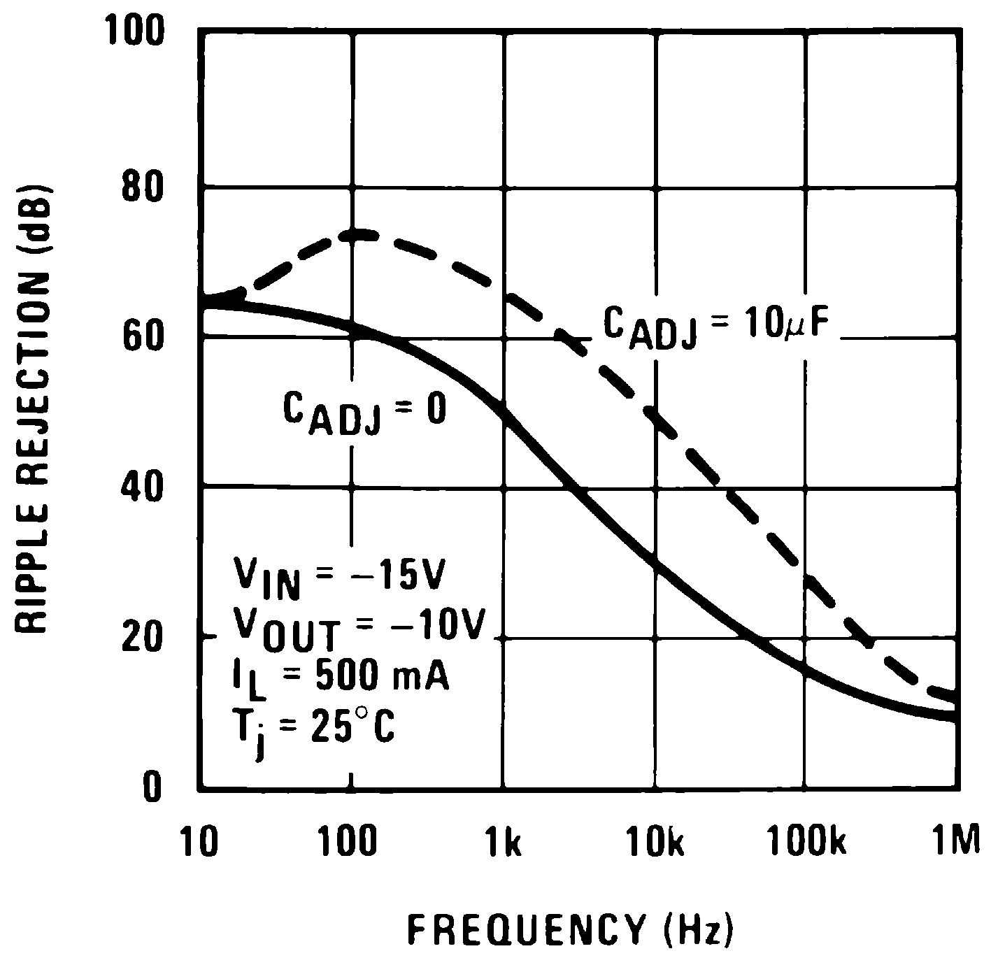
| Ripple rejection ratio | VOUT = −10 V, f = 120 Hz | 60 | 60 | dB | |||||
| CADJ = 10 μF | 66 | 77 | 66 | 77 | dB | ||||
| Long-term stability | TJ = 125°C, 1000 Hours | 0.3% | 1% | 0.3% | 1% | ||||
(1) Regulation is measured at constant junction temperature, using pulse testing with a low duty cycle. Changes in output voltage due to heating effects are covered under the specification for thermal regulation. Load regulation is measured on the output pin at a point ⅛ in. below the base of the TO packages.
(2) Selected devices with tightened tolerance reference voltage available.
6.6 Typical Characteristics
(NDE Package)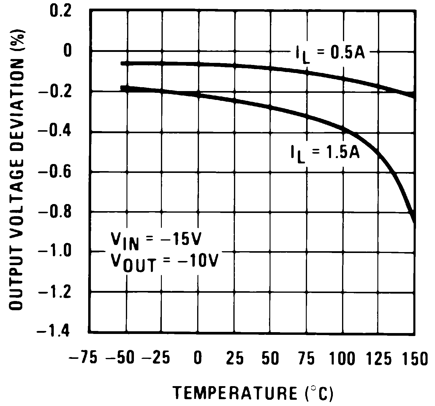 Figure 1. Load Regulation
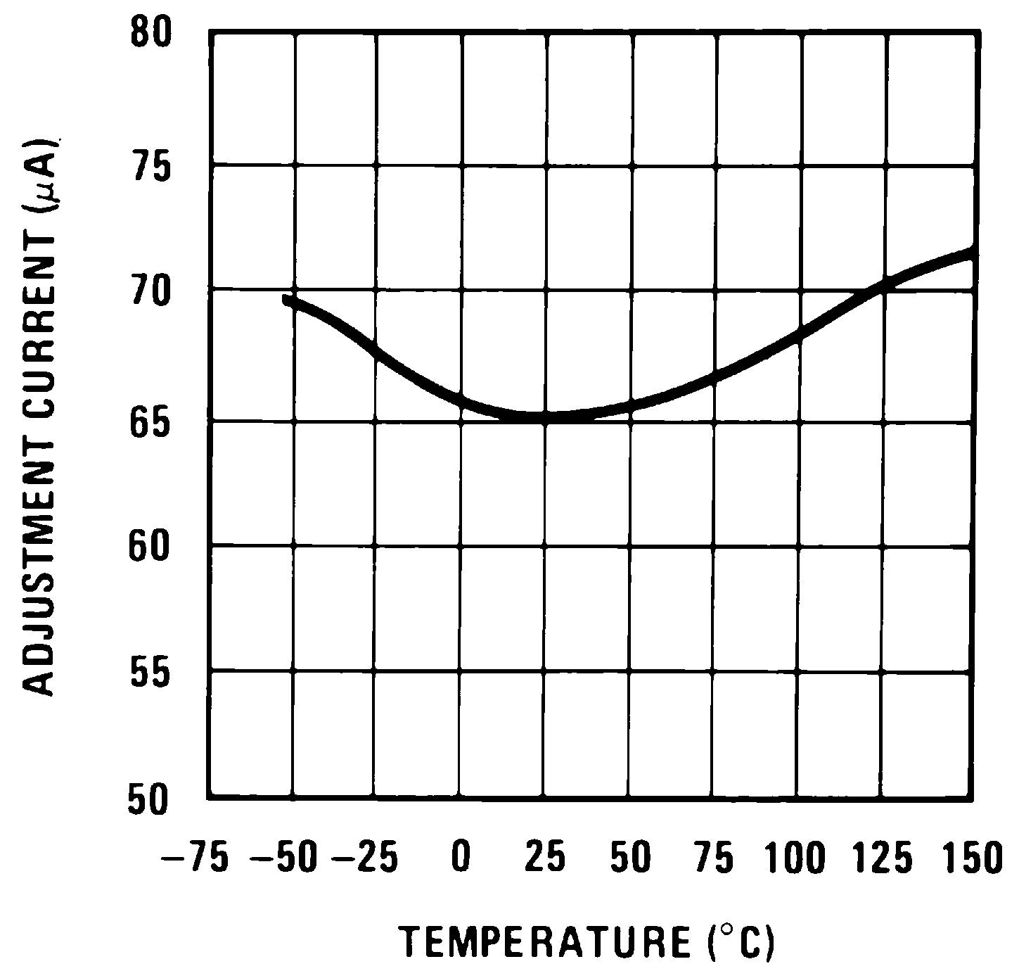 Figure 3. Adjustment Current
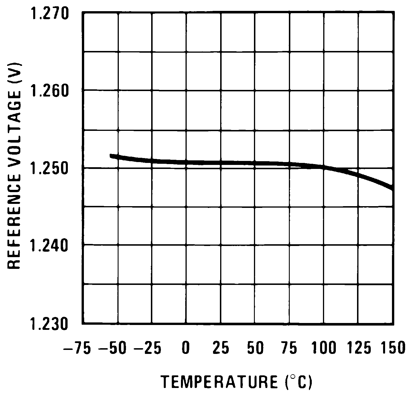 Figure 5. Temperature Stability
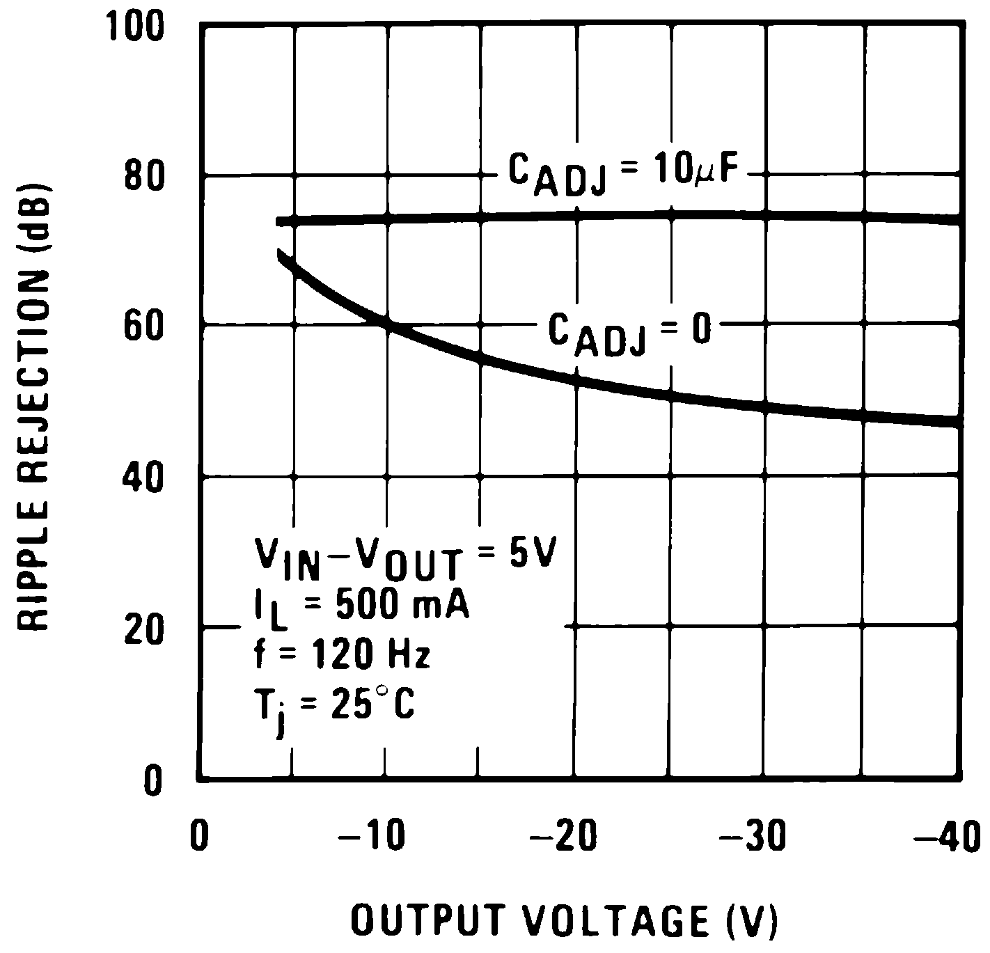 Figure 7. Ripple Rejection
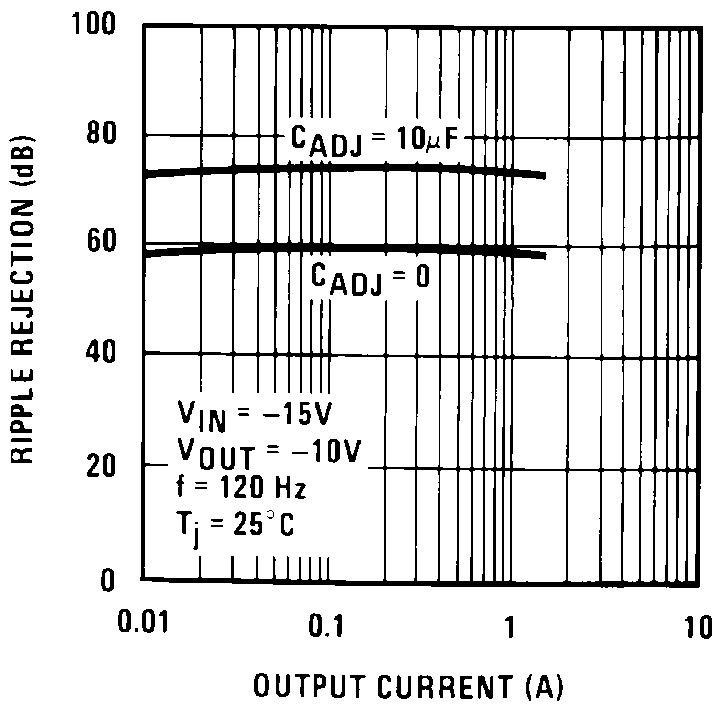 Figure 9. Ripple Rejection
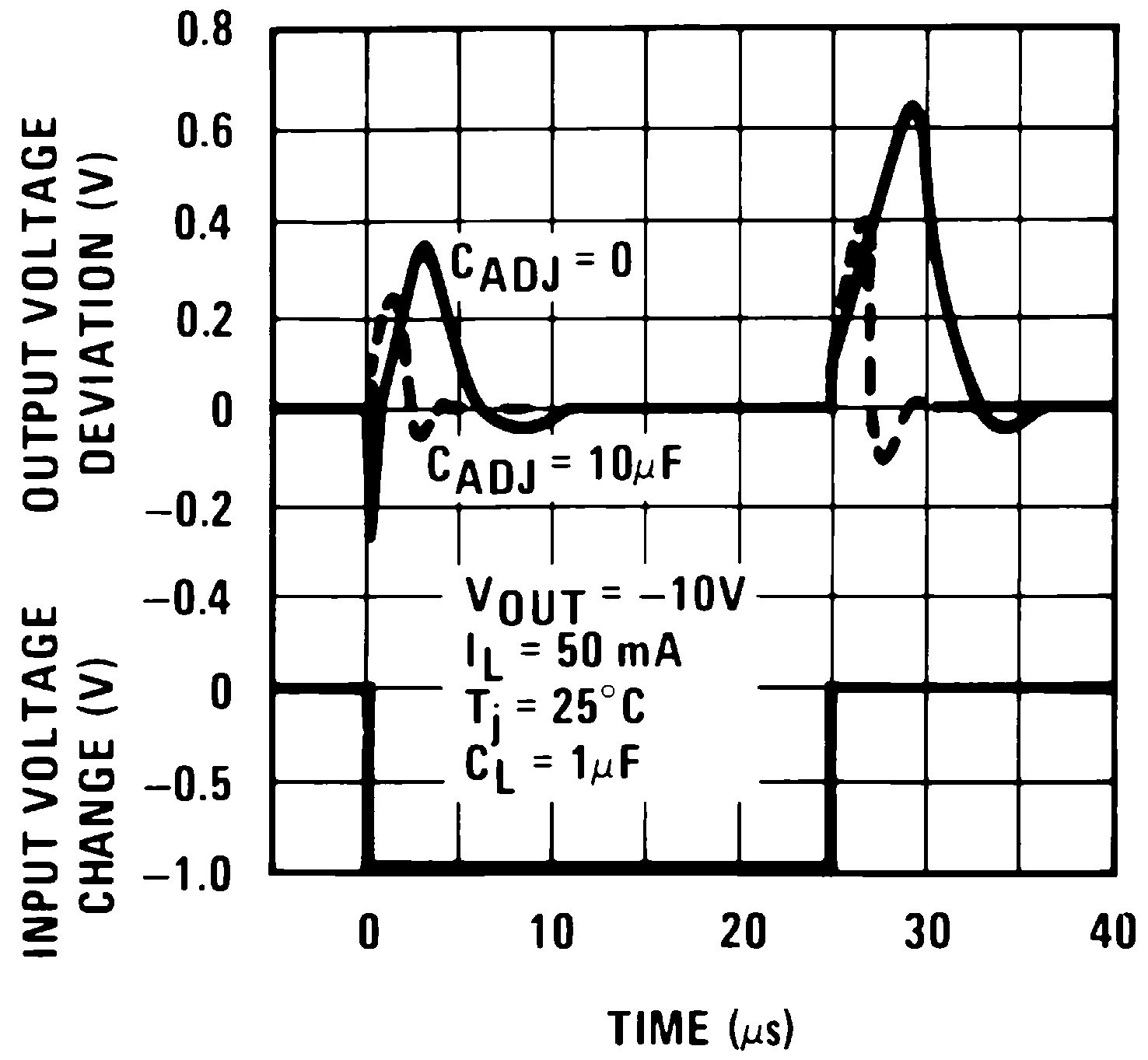 Figure 11. Line Transient Response
