ZHCSBI0C March 2013 – October 2014 LM3279
PRODUCTION DATA.
- 1 特性
- 2 应用
- 3 说明
- 4 修订历史记录
- 5 Pin Configuration and Functions
- 6 Specifications
- 7 Detailed Description
- 8 Application and Implementation
- 9 Power Supply Recommendations
- 10Layout
- 11器件和文档支持
- 12机械、封装和可订购信息
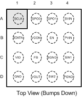
5 Pin Configuration and Functions
DSBGA
16 Pins

Pin Functions
| PIN | TYPE | DESCRIPTION | |
|---|---|---|---|
| NUMBER | NAME | ||
| A1 | SCLK | IN | Digital control interface (DCON) RFFE Bus clock input. Typically connected to RFFE master on RF or Baseband IC. SCLK must be held low when VIO is not applied. |
| B1 | SDATA | I/O | Digital control interface (DCON) RFFE Bus data input/output. Typically connected to RFFE master on RF or Baseband IC. SDATA must be held low when VIO is not applied. |
| C1 | VIO | IN | Digital control interface (DCON) 1.8-V supply input. VIO functions as the RFFE interface reference voltage. VIO also functions as a reset and enable input to LM3279. Bypass capacitor should be connected between VIO and GND. Typically connected to voltage regulator controlled by RF or Baseband IC. When VIO = HIGH, EN shall be connected to GND. |
| D1 | GND | Ground | Digital Ground. |
| A2 | GPO0 | I/O | Multipurpose GPIO. When VIO = HIGH, GPO0 is a general purpose output for configuring RF front end circuitry. When the GPO0 control bit in Register 02 is set to 1, the output is driven to a 1.8-V (VIO) high logic level. The output is pulled to a low logic level when the GPO0 control bit is set to 0. (Input has an internal pull-up resistor.) |
| B2 | VCON | IN | Voltage Control Analog input. When EN = HIGH, VCON controls the output voltage in PWM and PFM modes. When in Digital control, VCON can be left as no connect or connected to system ground. |
| C2 | FB | Ground | Feedback input to inverting input of error amplifier. Connect output voltage directly to this node at load point. |
| D2 | VOUT | PWR | Regulated output voltage of LM3279. Connect this to a 10-µF ceramic output filter capacitor to GND. |
| A3 | GPO1 | I/O | Multipurpose GPIO. When VIO = HIGH, GPO1 is a general purpose output for configuring RF front end circuitry. When the GPO1 control bit in Register 02 is set to 1, the output is driven to a 1.8-V (VIO) high logic level. The output is pulled to a low logic level when the GPO1 control bit is set to 0. (Input has an internal pull-up resistor.) |
| B3 | EN | IN | Enable Pin. Pulling this pin higher than 1.2 V enables part to function in analog control mode. VIO must be tied to ground. |
| C3 | SGND | Ground | Signal Ground for analog circuits and control circuitry. |
| D3 | SW2 | PWR | Switch pin for Internal Power Switches M3 and M4. Connect inductor between SW1 and SW2. |
| A4 | SVIN | PWR | SVIN is no connect. Analog supply is internally connected to PVIN. |
| B4 | PVIN | PWR | Power MOSFET input and power current input pin. Optional low-pass filtering may help reduce radiated EMI and noise during buck and buck-boost modes. |
| C4 | SW1 | PWR | Switch pin for Internal Power Switches M1 and M2. Connect inductor between SW1 and SW2. |
| D4 | PGND | Ground | Power Ground for Power MOSFETs and gate drive circuitry. |