SNVS793D November 2011 – May 2015 LM3269
PRODUCTION DATA.
- 1 Features
- 2 Applications
- 3 Description
- 4 Revision History
- 5 Pin Configuration and Functions
- 6 Specifications
- 7 Detailed Description
- 8 Application and Implementation
- 9 Power Supply Recommendations
- 10Layout
- 11Device and Documentation Support
- 12Mechanical, Packaging, and Orderable Information
8 Application and Implementation
NOTE
Information in the following applications sections is not part of the TI component specification, and TI does not warrant its accuracy or completeness. TI’s customers are responsible for determining suitability of components for their purposes. Customers should validate and test their design implementation to confirm system functionality.
8.1 Application Information
8.1.1 Setting The Output Voltage
The LM3269 features a pin-controlled variable output voltage which eliminates the need for external feedback resistors. It can be programmed for an output voltage from 0.6 V to 4.2 V by setting the voltage on the VCON pin, as in Equation 1.
When VCON is between 0.2 V and 1.4 V, the output voltage will follow the formula in Equation 1.
8.1.2 Output Current Capacity
The LM3269 load capability is as shown in Table 1.
Table 1. Output Voltage vs. Maximum Output Current Derating
| VOUT | VBATT | MAXIMUM IOUT CAPABILITY |
|---|---|---|
| 4.2 V | > 3 V | 650 mA |
| 2.7 V to 3 V | 500 mA | |
| 3.8 V | > 3 V | 750 mA |
| 2.7 V to 3 V | 600 mA | |
| < 1.5 V | 2.7 V to 5.5 V | 120 mA (in PFM mode) |
8.2 Typical Application
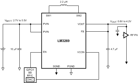
8.2.1 Design Requirements
| DESIGN PARAMETER | EXAMPLE VALUE |
|---|---|
| Minimum input voltage | 2.7 V |
| Minimum output voltage | 0.6 V |
| Output current | 0 to 750 mA |
| Switching frequency | 2.4 MHz (typical) |
8.2.2 Detailed Design Procedure
8.2.2.1 Recommended External Components
8.2.2.1.1 Inductor Selection
A 2.2-μH inductor with a saturation current rating over 1500 mA and low inductance drop at the full DC bias condition is recommended for almost all applications. An inductor with a smaller DC resistance, such as 110 mΩ (depending on case size of resistor), should be used for good efficiency.
Table 2. Suggested 2.2-µH Inductors
| VENDOR | MODEL | DIMENSIONS (mm) | ISAT
(30% drop) |
IRATING
(Δ40°) |
DCR |
|---|---|---|---|---|---|
| FDK | MIPSZ2520D2R2 | 2.5 x 2.0 x 1.0 | 1.5 A | 1.1 A | 110 mΩ |
| Murata | LQH2HPN1R0NG0 | 2.5 x 2.0 x 1.2 | 2 A | 1.2 A | 112 mΩ |
| Samsung | CIG22H2R2MNE | 2.5 x 2.0 x 1.2 | 1.9 A | 1.6 A | 116 mΩ |
| TDK | TFM201610A2R2M | 2.0 x 1.6 x 1.0 | 1.7 A | 1.3 A | 180 mΩ |
| TOKO | DFE201612C2R2N | 2.0 x 1.6 x 1.2 | 2.1 A | 1.3 A | 155 mΩ |
8.2.2.1.2 Input Capacitor Selection
A ceramic input capacitor of 10 µF, 6.3 V, 0603 (1608) is recommended for use in most applications. Place the input capacitor as close as possible to the PVIN pin and PGND pin of the device. A larger value of higher voltage rating may be used to improve input filtering. Use X7R, X5R, or B types; do not use Y5V or F. DC board characteristics of ceramic capacitors must be considered when selecting case sizes like 0402 (1005). The input filter capacitor supplies current to the PFET (high-side) switch in first half of each cycle and reduces voltage ripple imposed on the input power source. A ceramic capacitor’s low equivalent series resistance (ESR) provides the best noise filtering of the input voltage spikes due to this rapidly changing current.
8.2.2.1.3 Output Capacitor Selection
Use a 4.7 µF capacitor for the output capacitor. Use of capacitor types such as X5R, X7R are recommended for the filter. These provide an optimal balance between small size, cost, reliability, and performance for cell phones and similar applications. Table 3 lists suggested part numbers and suppliers. DC bias characteristics of the capacitors must be considered while selecting the voltage rating and case size of the capacitor. Smaller case sizes for the output capacitor mitigate piezo-electric vibrations of the capacitor when the output voltage is stepped up and down at fast rates. However, they have a bigger percentage drop in value with DC bias. A 0603 (1608) case size capacitor is recommended for output. For RF Power Amplifier applications, split the output capacitor between DC-DC converter and RF Power Amplifier(s). (4.7 μF (0402 (1005)) + PA input cap (0402(1005)/0201(0603)) is recommended.) The optimum capacitance split is application dependent. Place all the output capacitors very close to their respective device.
NOTE
If using a 4.7 µF, 0402 (1005) as the output capacitor, the total recommended actual capacitance on VOUT bus should be at least 7 µF (4.7 µF + PA decoupling caps) to take into account the 0402 (1005) DC bias degradation and other tolerances.
Table 3. Suggested Capacitors
| MODEL | VENDOR |
|---|---|
| 10 µF for CIN | |
| C1608X5R0J106K (0603) | TDK |
| CL05A106MQ5NUN (0402) | Samsung |
| 4.7 µF for COUT | |
| C1608X5R0J475M (0603) | TDK |
| CL05A475MQ5NRN (0402) | Samsung |
| C1005X5RR0J475M (0402) | TDK |
8.2.3 Application Curves
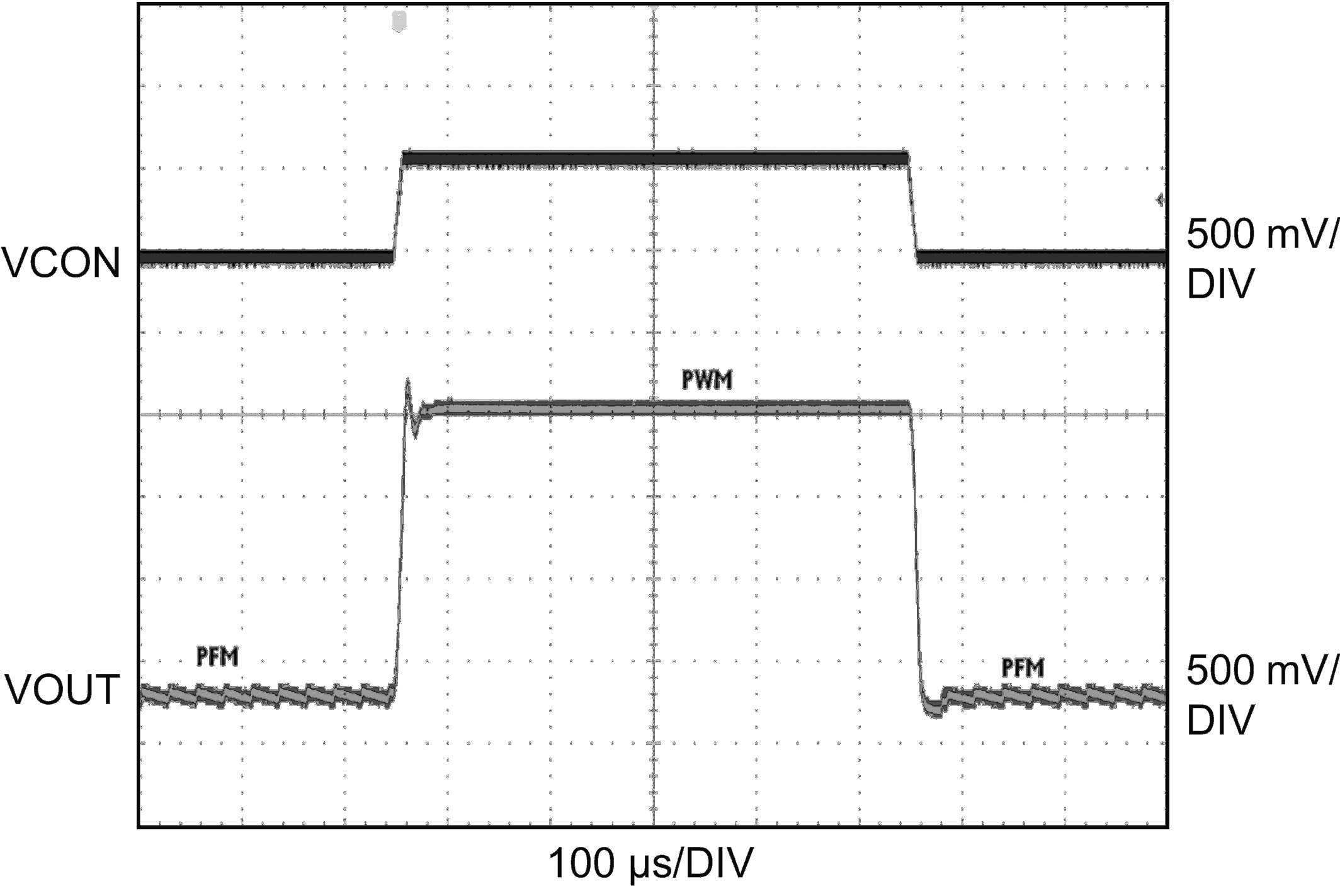
| PVIN = 3.7 V | VOUT = 0.8 V↔ 2 V | RLOAD = 20 Ω |
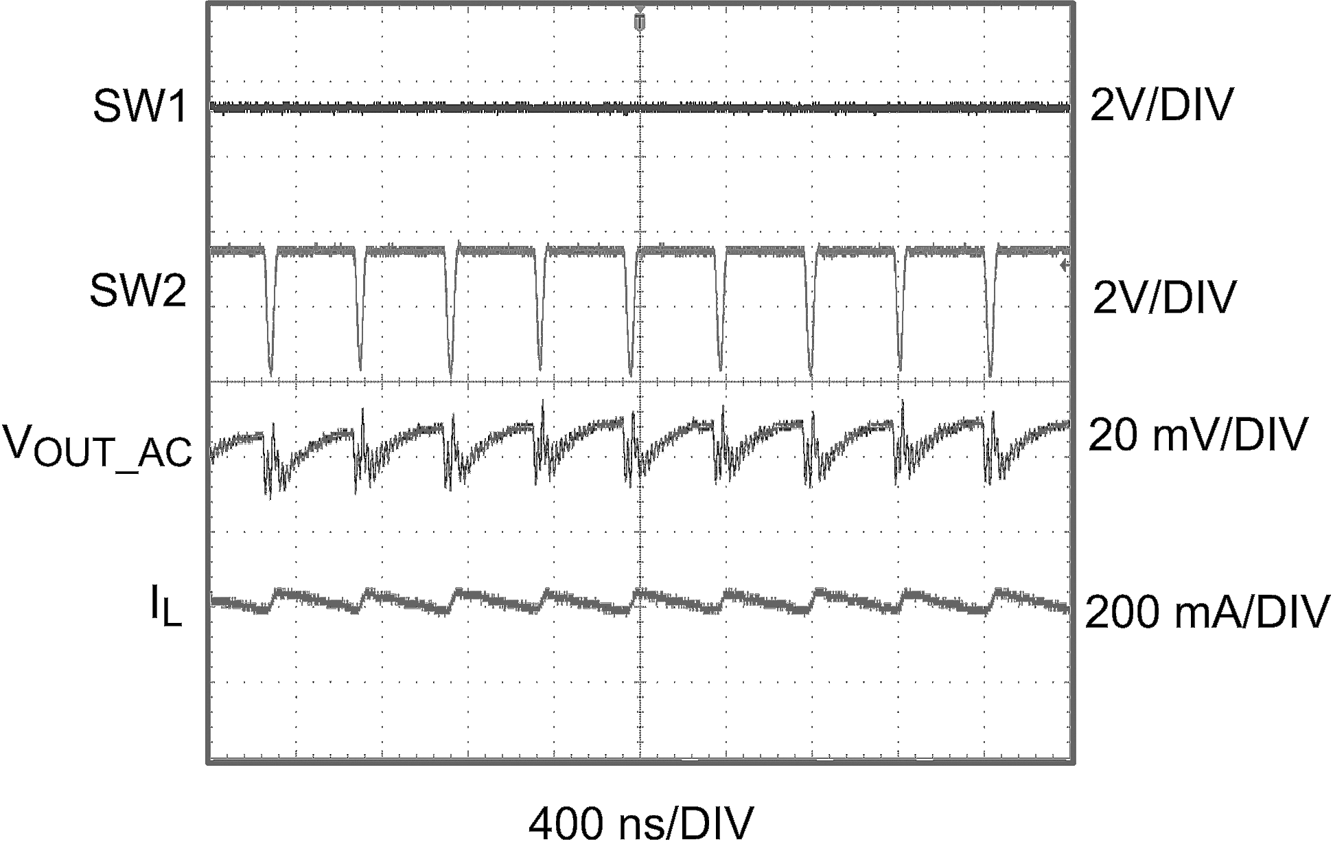
| PVIN = 3.37 V | VOUT = 3.45 V | Load = 500 mA |
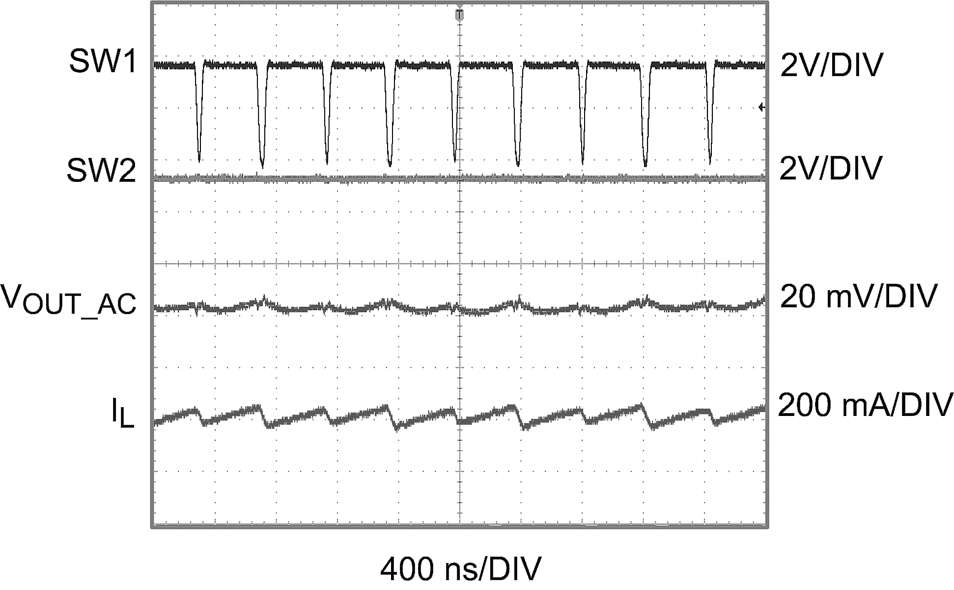
| PVIN= 3.7 V | VOUT = 3.2 V | Load = 500 mA |
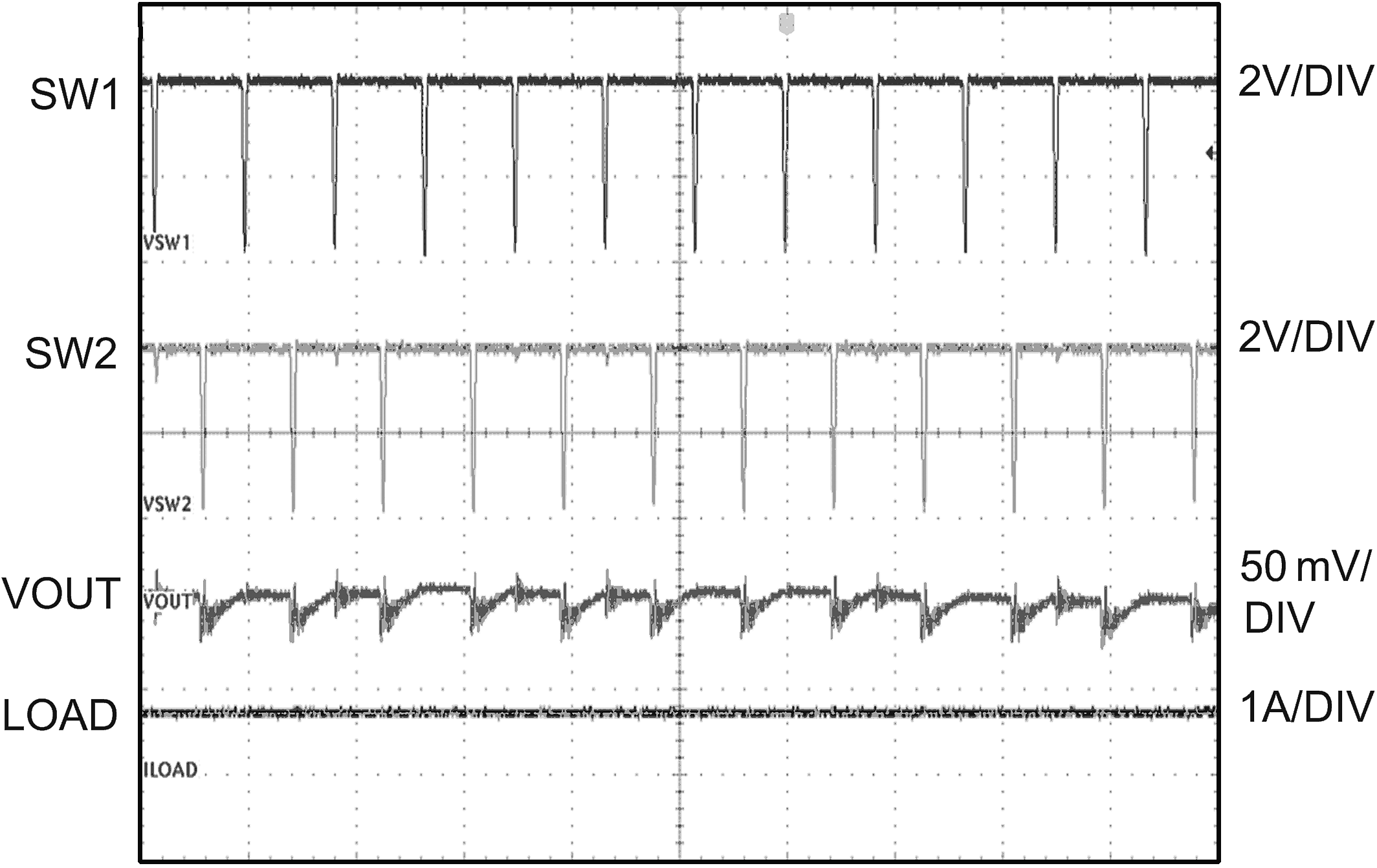
| PVIN = 3.8 V | VOUT = 3.6 V | IOUT = 600 mA |
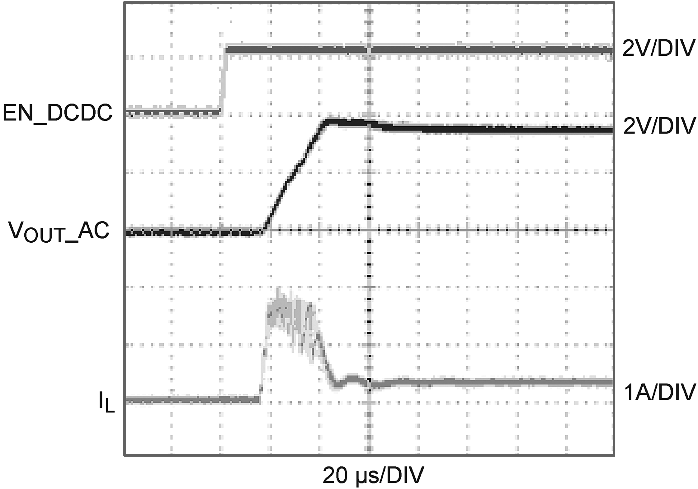
| PVIN = 3.6 V | VOUT = 3.45 V | Load = 350 mA |
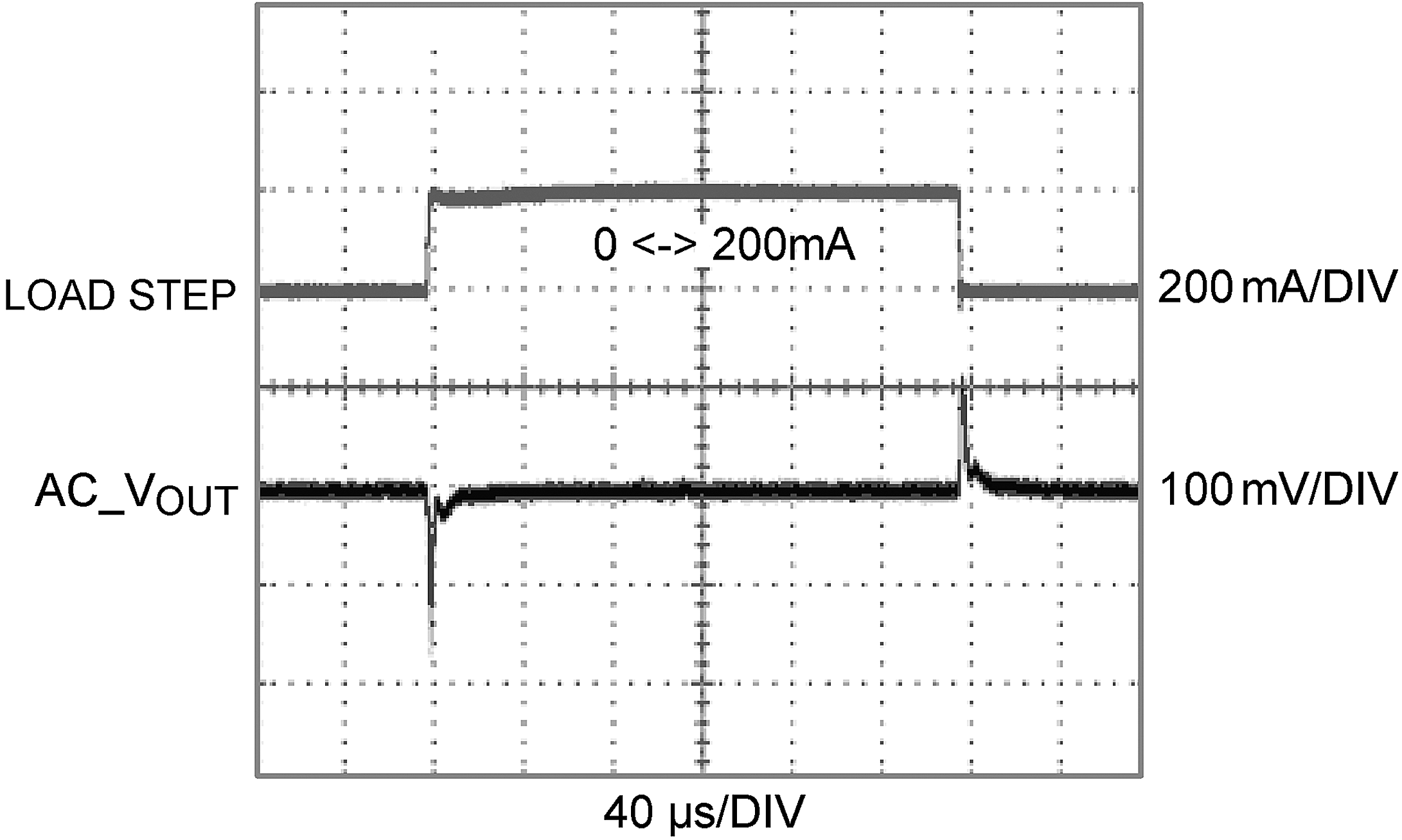
| PVIN = 3.8 V | VOUT = 3.45 V | |
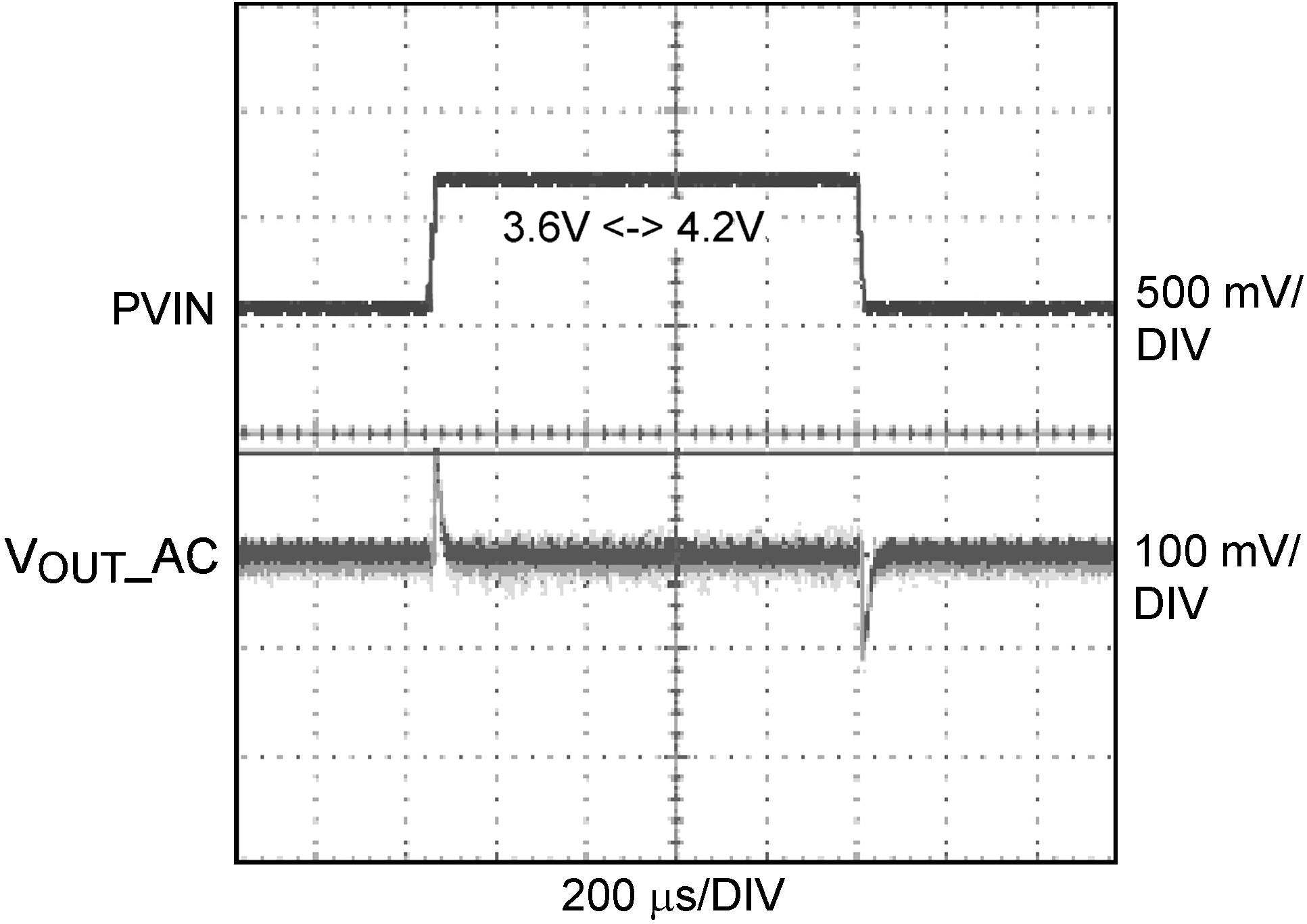
| PVIN Step = 3.6 V ↔ 4.2 V | VOUT = 3 V | Load = 320 mA |