SNVS769J March 2000 – December 2014 LM2940-N , LM2940C
PRODUCTION DATA.
- 1 Features
- 2 Applications
- 3 Description
- 4 Revision History
- 5 Pin Configuration and Functions
- 6 Specifications
- 7 Detailed Description
- 8 Application and Implementation
- 9 Power Supply Recommendations
- 10Layout
- 11Device and Documentation Support
- 12Mechanical, Packaging, and Orderable Information
封装选项
请参考 PDF 数据表获取器件具体的封装图。
机械数据 (封装 | 引脚)
- NDE|3
- NGN|8
- DCY|4
- KTT|3
- NEB|3
散热焊盘机械数据 (封装 | 引脚)
订购信息
6 Specifications
6.1 Absolute Maximum Ratings(1)(4)
| MIN | MAX | UNIT | ||
|---|---|---|---|---|
| LM2940-N KTT, NDE, DCY ≤ 100 ms | 60 | V | ||
| LM2940C KTT, NDE ≤ 1 ms | 45 | |||
| Internal power dissipation(2) | Internally Limited | |||
| Maximum junction temperature | 150 | °C | ||
| Soldering temperature(3) | TO-220 (NDE), Wave (10 s) | 260 | ||
| DDPAK/TO-263 (KTT) (30 s) | 235 | |||
| SOT-223 (DCY) (30 s) | 260 | |||
| WSON-8 (NGN) (30 s) | 235 | |||
| Storage temperature, Tstg | −65 | 150 | ||
(1) Absolute Maximum Ratings are limits beyond which damage to the device may occur. Recommended Operating Conditions are conditions under which the device functions but the specifications might not be ensured. For ensured specifications and test conditions see the Electrical Characteristics (5 V and 8 V).
(2) The maximum allowable power dissipation is a function of the maximum junction temperature, TJ, the junction-to-ambient thermal resistance, RθJA, and the ambient temperature, TA. Exceeding the maximum allowable power dissipation will cause excessive die temperature, and the regulator will go into thermal shutdown. The value of R θJA (for devices in still air with no heatsink) is 23.3°C/W for the TO-220 package, 40.9°C/W for the DDPAK/TO-263 package, and 59.3°C/W for the SOT-223 package. The effective value of RθJA can be reduced by using a heatsink (see Heatsinking for specific information on heatsinking). The value of RθJA for the WSON package is specifically dependent on PCB trace area, trace material, and the number of layers and thermal vias. For improved thermal resistance and power dissipation for the WSON package, refer to Application Note AN-1187 Leadless Leadframe Package (LLP) (SNOA401). It is recommended that 6 vias be placed under the center pad to improve thermal performance.
(3) Refer to JEDEC J-STD-020C for surface mount device (SMD) package reflow profiles and conditions. Unless otherwise stated, the temperature and time are for Sn-Pb (STD) only.
(4) If Military/Aerospace specified devices are required, please contact the Texas Instruments Sales Office/ Distributors for availability and specifications.
6.2 ESD Ratings
| VALUE | UNIT | |||
|---|---|---|---|---|
| V(ESD) | Electrostatic discharge | Human-body model (HBM), per ANSI/ESDA/JEDEC JS-001(1) | ±2000 | V |
(1) JEDEC document JEP155 states that 500-V HBM allows safe manufacturing with a standard ESD control process.
6.3 Recommended Operating Conditions
over operating free-air temperature range (unless otherwise noted)| MIN | MAX | UNIT | ||
|---|---|---|---|---|
| Input voltage | 6 | 26 | V | |
| Temperature | LM2940-N NDE, LM2940-N KTT | −40 | 125 | °C |
| LM2940C NDE, LM2940C KTT | 0 | 125 | ||
| LM2940-N DCY | −40 | 85 | ||
| LM2940-N NGN | −40 | 125 | ||
6.4 Thermal Information
| THERMAL METRIC(1) | LM2940-N, LM2940C | LM2940-N | UNIT | |||
|---|---|---|---|---|---|---|
| TO-220 (NDE) | DDPAK/TO-263 (KTT) | SOT-223 (DCY) | WSON (NGN) | |||
| 3 PINS | 3 PINS | 4 PINS | 8 PINS | |||
| RθJA | Junction-to-ambient thermal resistance(2) | 23.3 | 40.9 | 59.3 | 40.5 | °C/W |
| RθJC(top) | Junction-to-case (top) thermal resistance | 16.1 | 43.5 | 38.9 | 26.2 | |
| RθJB | Junction-to-board thermal resistance | 4.8 | 23.5 | 8.1 | 17.0 | |
| ψJT | Junction-to-top characterization parameter | 2.7 | 10.3 | 1.7 | 0.2 | |
| ψJB | Junction-to-board characterization parameter | 4.8 | 22.5 | 8.0 | 17.2 | |
| RθJC(bot) | Junction-to-case (bottom) thermal resistance | 1.1 | 0.8 | n/a | 3.2 | |
(1) For more information about traditional and new thermal metrics, see the IC Package Thermal Metrics application report, SPRA953.
(2) Thermal information for the TO-220 package is for a package vertically mounted with a heat sink in the middle of a PCB which is compliant to the JEDEC HIGH-K 2s2p (JESD51-7). The heatsink-to-ambient thermal resistance, RƟSA, is 21.7°C/W. See Heatsinking TO-220 Package Parts for more information.
6.5 Electrical Characteristics (5 V and 8 V)
Unless otherwise specified: VIN = VOUT + 5 V, IOUT = 1 A and COUT = 22 µF. MIN (minimum) and MAX (maximum) limits apply over the recommended operating temperature range, unless otherwise noted; typical limits apply for TA = TJ = 25°C.| PARAMETER | TEST CONDITIONS | 5 V | 8 V | UNIT | |||||
|---|---|---|---|---|---|---|---|---|---|
| MIN | TYP | MAX | MIN | TYP | MAX | ||||
| Input voltage | 5 mA ≤ IOUT ≤ 1 A | 6.25 | 26 | 9.4 | 26 | V | |||
| Output voltage | 5 mA ≤ IOUT ≤ 1A | 4.75 | 5 | 5.25 | 7.6 | 8 | 8.4 | ||
| 5 mA ≤ IOUT ≤ 1A, TJ = 25°C | 4.85 | 5 | 5.15 | 7.76 | 8 | 8.24 | |||
| Line regulation | VOUT + 2 V ≤ VIN ≤ 26 V, IOUT = 5 mA TJ = 25°C |
20 | 50 | 20 | 80 | mV | |||
| Load regulation | 50 mA ≤ IOUT ≤ 1 A | LM2940-N | 35 | 80 | 55 | 130 | mV | ||
| 50 mA ≤ IOUT ≤ 1 A TJ = 25°C |
LM2940-N | 35 | 50 | 55 | 80 | ||||
| LM2940C | 35 | 50 | 55 | 80 | |||||
| Output impedance | 100 mADC, 20 mArms, ƒOUT = 120 Hz | 35 | 55 | mΩ | |||||
| Quiescent current | VOUT + 2 V ≤ VIN ≤ 26 V, IOUT = 5 mA |
LM2940-N | 10 | 20 | 10 | 20 | mA | ||
| VOUT + 2 V ≤ VIN ≤ 26 V, IOUT = 5 mA TJ = 25°C |
LM2940-N | 10 | 15 | 10 | 15 | ||||
| LM2940C | 10 | 15 | |||||||
| VIN = VOUT + 5 V, IOUT = 1 A | 30 | 60 | 30 | 60 | |||||
| VIN = VOUT + 5 V, IOUT = 1 A TJ = 25°C |
30 | 45 | 30 | 45 | |||||
| Output noise voltage | 10 Hz to 100 kHz, IOUT = 5 mA | 150 | 240 | µVrms | |||||
| Ripple rejection | ƒOUT = 120 Hz, 1 Vrms, IOUT = 100 mA | LM2940-N | 54 | 72 | 48 | 66 | dB | ||
| ƒOUT = 120 Hz, 1 Vrms, IOUT = 100 mA TJ = 25°C |
LM2940-N | 60 | 72 | 54 | 66 | ||||
| LM2940C | 60 | 72 | 54 | 66 | |||||
| Long-term stability | 20 | 32 | mV/1000 Hr | ||||||
| Dropout voltage | IOUT = 1A | 0.5 | 1 | 0.5 | 1 | V | |||
| IOUT = 1A, TJ = 25°C | 0.5 | 0.8 | 0.5 | 0.8 | |||||
| IOUT = 100 mA | 110 | 200 | 110 | 200 | mV | ||||
| IOUT = 100 mA, TJ = 25°C | 110 | 150 | 110 | 150 | |||||
| Short-circuit current | See(1), TJ = 25°C | 1.6 | 1.9 | 1.6 | 1.9 | A | |||
| Maximum line transient | ROUT = 100Ω, T ≤ 100 ms | LM2940-N | 60 | 75 | 60 | 75 | V | ||
| ROUT = 100Ω, T ≤ 1 ms TJ = 25°C |
LM2940C | 45 | 55 | 45 | 555 | ||||
| Reverse polarity DC input voltage |
ROUT = 100 Ω | LM2940-N | –15 | –30 | –15 | –30 | V | ||
| ROUT = 100 Ω TJ = 25°C |
LM2940C | –15 | –30 | –15 | –30 | ||||
| Reverse polarity Transient Input Voltage |
ROUT = 100 Ω, T ≤ 100 ms | LM2940-N | –50 | –75 | –50 | –75 | V | ||
| ROUT = 100 Ω, T ≤ 1 ms | LM2940C | –45 | –55 | ||||||
(1) Output current will decrease with increasing temperature but will not drop below 1 A at the maximum specified temperature.
6.6 Electrical Characteristics (9 V and 10 V)
Unless otherwise specified: VIN = VOUT + 5 V, IOUT = 1 A and COUT = 22 µF. MIN (minimum) and MAX (maximum) limits apply over the recommended operating temperature range, unless otherwise noted; typical limits apply for TA = TJ = 25°C.| PARAMETER | TEST CONDITIONS | 9 V | 10 V | UNIT | |||||
|---|---|---|---|---|---|---|---|---|---|
| MIN | TYP | MAX | MIN | TYP | MAX | ||||
| Input voltage | 5 mA ≤ IOUT ≤ 1 A | 10.5 | 26 | 11.5 | 26 | V | |||
| Output voltage | 5 mA ≤ IOUT ≤ 1A | 8.55 | 9 | 9.45 | 9.5 | 10 | 10.5 | ||
| 5 mA ≤ IOUT ≤ 1A, TJ = 25°C | 8.73 | 9 | 9.27 | 9.7 | 10 | 10.3 | |||
| Line regulation | VOUT + 2 V ≤ VIN ≤ 26 V, IOUT = 5 mA TJ = 25°C |
20 | 90 | 20 | 100 | mV | |||
| Load regulation | 50 mA ≤ IOUT ≤ 1 A | LM2940-N | 60 | 150 | 65 | 165 | mV | ||
| 50 mA ≤ IOUT ≤ 1 A TJ = 25°C |
LM2940-N | 60 | 90 | 65 | 100 | ||||
| LM2940C | 60 | 90 | |||||||
| Output impedance | 100 mADC, 20 mArms, ƒOUT = 120 Hz | 60 | 65 | mΩ | |||||
| Quiescent current | VOUT + 2 V ≤ VIN ≤ 26 V, IOUT = 5 mA |
LM2940-N | 10 | 20 | 10 | 20 | mA | ||
| VOUT + 2 V ≤ VIN ≤ 26 V, IOUT = 5 mA TJ = 25°C |
LM2940-N | 10 | 15 | 15 | |||||
| LM2940C | 10 | 15 | |||||||
| VIN = VOUT + 5 V, IOUT = 1 A | 30 | 60 | 30 | 60 | |||||
| VIN = VOUT + 5 V, IOUT = 1 A TJ = 25°C |
30 | 45 | 30 | 45 | |||||
| Output noise voltage | 10 Hz to 100 kHz, IOUT = 5 mA | 270 | 300 | µVrms | |||||
| Ripple rejection | ƒOUT = 120 Hz, 1 Vrms
IOUT = 100 mA |
LM2940-N | 46 | 64 | 45 | 63 | dB | ||
| ƒOUT = 120 Hz, 1 Vrms
IOUT = 100 mA TJ = 25°C |
LM2940-N | 52 | 64 | 51 | 63 | ||||
| LM2940C | 52 | 64 | |||||||
| Long-term stability | 34 | 36 | mV/1000 Hr | ||||||
| Dropout voltage | IOUT = 1A | 0.5 | 1 | 0.5 | 1 | V | |||
| IOUT = 1A, TJ = 25°C | 0.5 | 0.8 | 0.5 | 0.8 | |||||
| IOUT = 100 mA | 110 | 200 | 110 | 200 | mV | ||||
| IOUT = 100 mA, TJ = 25°C | 110 | 150 | 110 | 150 | |||||
| Short-circuit current | See(1), TJ = 25°C | 1.6 | 1.9 | 1.6 | 1.9 | A | |||
| Maximum line transient | ROUT = 100Ω, T ≤ 100 ms | LM2940-N | 60 | 75 | 60 | 75 | V | ||
| ROUT = 100Ω, T ≤ 100 ms TJ = 25°C |
LM2940C | 45 | 55 | ||||||
| Reverse polarity DC input voltage |
ROUT = 100 Ω | LM2940-N | –15 | –30 | –15 | –30 | V | ||
| ROUT = 100 Ω TJ = 25°C |
LM2940C | –15 | –30 | ||||||
| Reverse polarity Transient Input Voltage |
ROUT = 100 Ω, T ≤ 100 ms | LM2940-N | –50 | –75 | –50 | –75 | V | ||
| LM2940C | –45 | –55 | |||||||
6.7 Electrical Characteristics (12 V and 15 V)
Unless otherwise specified: VIN = VOUT + 5 V, IOUT = 1 A and COUT = 22 µF. MIN (minimum) and MAX (maximum) limits apply over the recommended operating temperature range, unless otherwise noted; typical limits apply for TA = TJ = 25°C.| PARAMETER | TEST CONDITIONS | 12 V | 15 V | UNIT | |||||
|---|---|---|---|---|---|---|---|---|---|
| MIN | TYP | MAX | MIN | TYP | MAX | ||||
| Input voltage | 5 mA ≤ IOUT ≤ 1 A | 13.6 | 26 | 16.75 | 26 | V | |||
| Output voltage | 5 mA ≤ IOUT ≤ 1A | 11.40 | 12 | 12.6 | 14.25 | 15 | 15.75 | ||
| 5 mA ≤ IOUT ≤ 1A, TJ = 25°C | 11.64 | 12 | 12.36 | 14.55 | 15 | 15.45 | |||
| Line regulation | VOUT + 2 V ≤ VIN ≤ 26 V, IOUT = 5 mA TJ = 25°C |
20 | 120 | 20 | 150 | mV | |||
| Load regulation | 50 mA ≤ IOUT ≤ 1 A | LM2940-N | 55 | 200 | mV | ||||
| 50 mA ≤ IOUT ≤ 1 A TJ = 25°C |
LM2940-N | 55 | 120 | ||||||
| LM2940C | 55 | 120 | 70 | 150 | |||||
| Output impedance | 100 mADC, 20 mArms, ƒOUT = 120 Hz | 80 | 100 | mΩ | |||||
| Quiescent current | VOUT + 2 V ≤ VIN ≤ 26 V, IOUT = 5 mA |
LM2940-N | 10 | 20 | mA | ||||
| VOUT + 2 V ≤ VIN ≤ 26 V, IOUT = 5 mA TJ = 25°C |
LM2940-N | 10 | 15 | ||||||
| LM2940C | 10 | 15 | 10 | 15 | |||||
| VIN = VOUT + 5 V, IOUT = 1 A | 30 | 60 | 30 | 60 | |||||
| VIN = VOUT + 5 V, IOUT = 1 A TJ = 25°C |
30 | 45 | 30 | 45 | |||||
| Output noise voltage | 10 Hz to 100 kHz, IOUT = 5 mA | 360 | 450 | µVrms | |||||
| Ripple rejection | ƒOUT = 120 Hz, 1 Vrms, IOUT = 100 mA | LM2940-N | 48 | 66 | dB | ||||
| ƒOUT = 120 Hz, 1 Vrms, IOUT = 100 mA TJ = 25°C |
LM2940-N | 54 | 66 | ||||||
| LM2940C | 54 | 66 | 52 | 64 | |||||
| Long-term stability | 48 | 60 | mV/1000 Hr | ||||||
| Dropout voltage | IOUT = 1A | 0.5 | 1 | 0.5 | 1 | V | |||
| IOUT = 1A, TJ = 25°C | 0.5 | 0.8 | 0.5 | 0.8 | |||||
| IOUT = 100 mA | 110 | 200 | 110 | 200 | mV | ||||
| IOUT = 100 mA, TJ = 25°C | 110 | 150 | 110 | 150 | |||||
| Short-circuit current | See(1), TJ = 25°C | 1.6 | 1.9 | 1.6 | 1.9 | A | |||
| Maximum line transient | ROUT = 100Ω, T ≤ 100 ms | LM2940-N | 60 | 75 | V | ||||
| ROUT = 100Ω, T ≤ 100 ms TJ = 25°C |
LM2940C | 45 | 55 | 45 | 55 | ||||
| Reverse polarity DC input voltage |
ROUT = 100 Ω | LM2940-N | –15 | –30 | V | ||||
| ROUT = 100 Ω TJ = 25°C |
LM2940C | –15 | –30 | –15 | –30 | ||||
| Reverse polarity transient input voltage |
ROUT = 100 Ω, T ≤ 100 ms | LM2940-N | –50 | –75 | V | ||||
| ROUT = 100 Ω, T ≤ 1 ms | LM2940C | –45 | –55 | –45 | –55 | ||||
6.8 Typical Characteristics
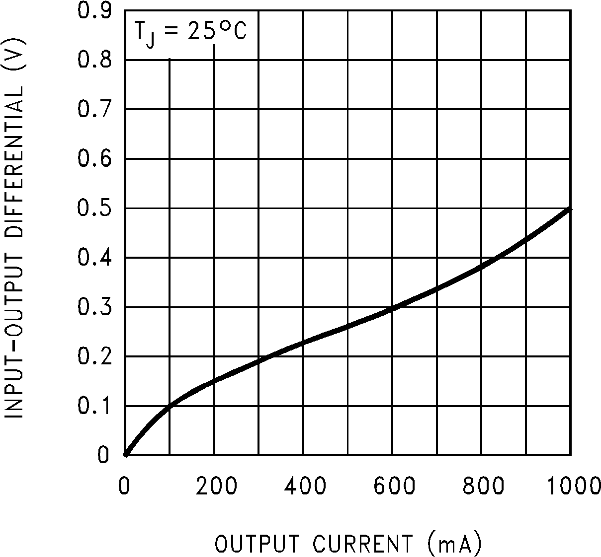 Figure 1. Dropout Voltage
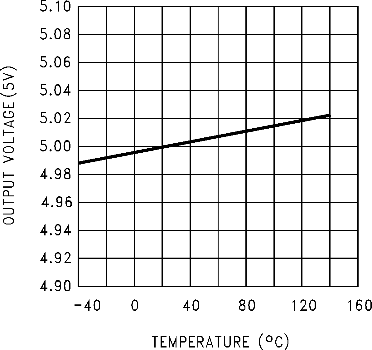 Figure 3. Output Voltage vs. Temperature
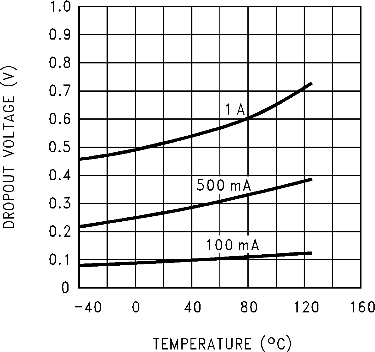 Figure 2. Dropout Voltage vs. Temperature
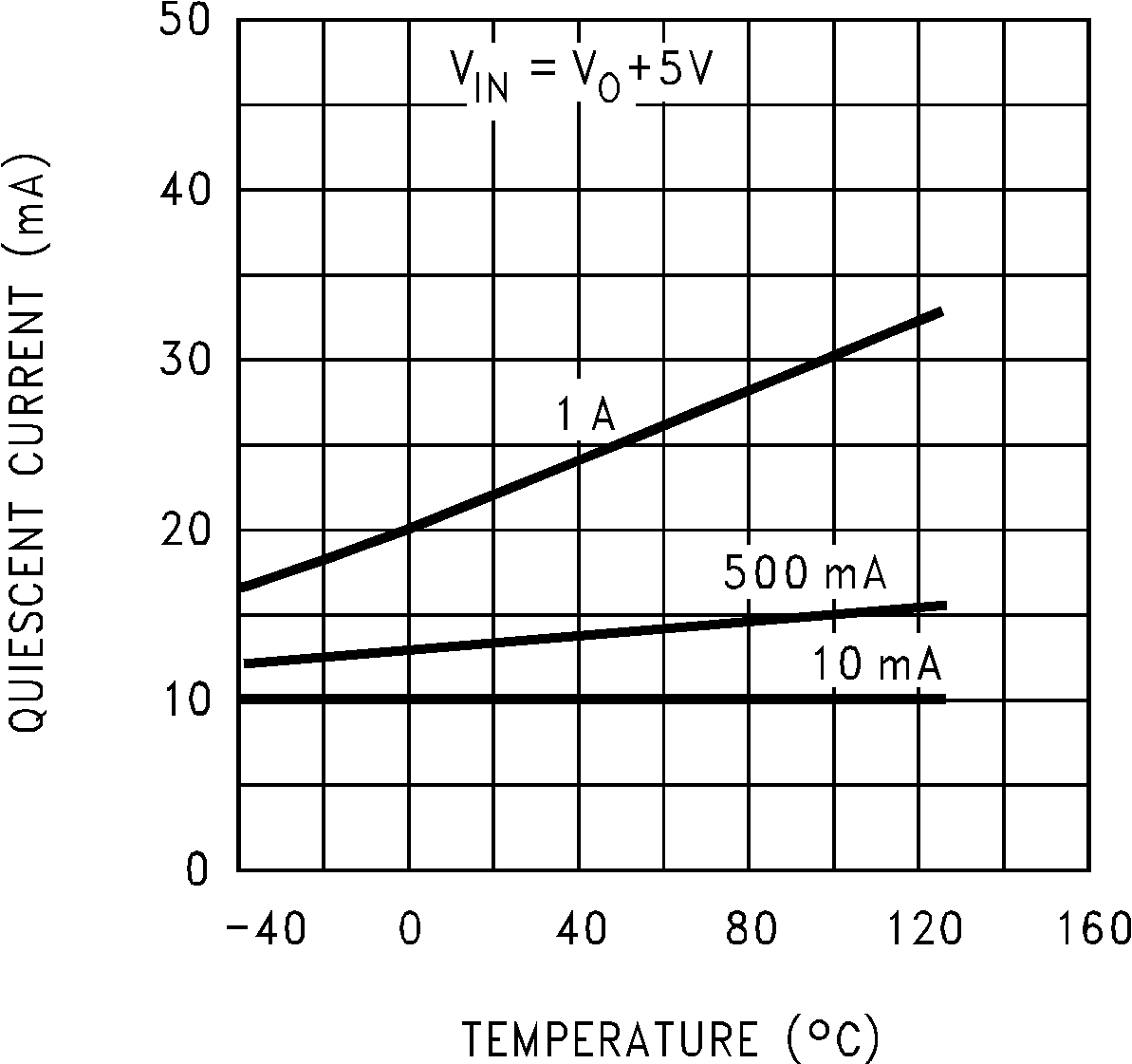 Figure 4. Quiescent Current vs. Temperature
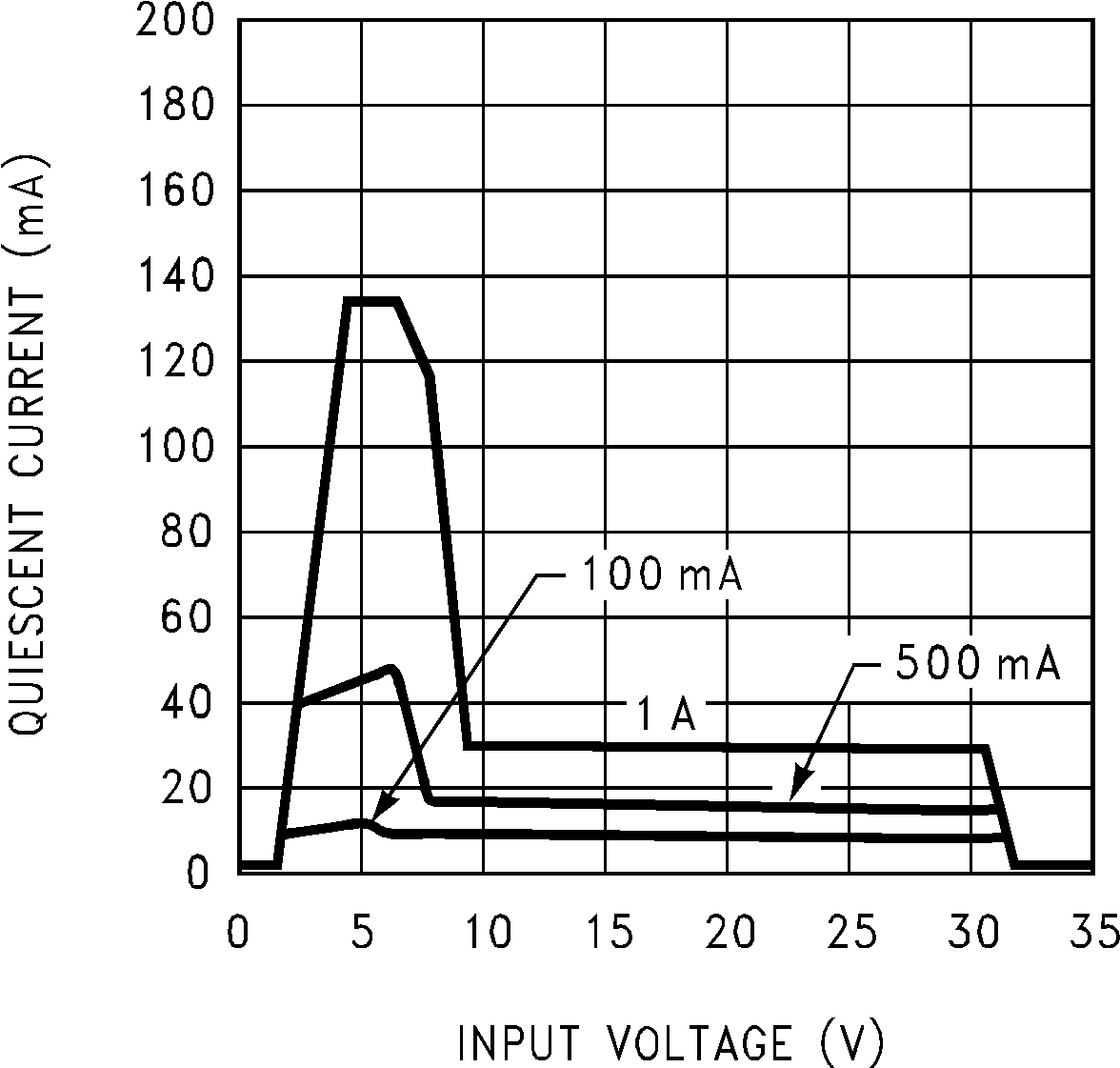 Figure 5. Quiescent Current
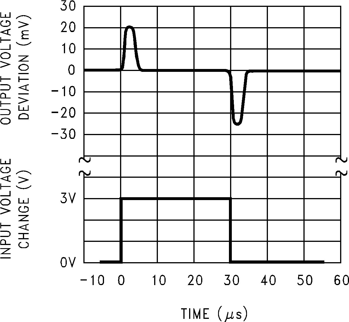 Figure 7. Line Transient Response
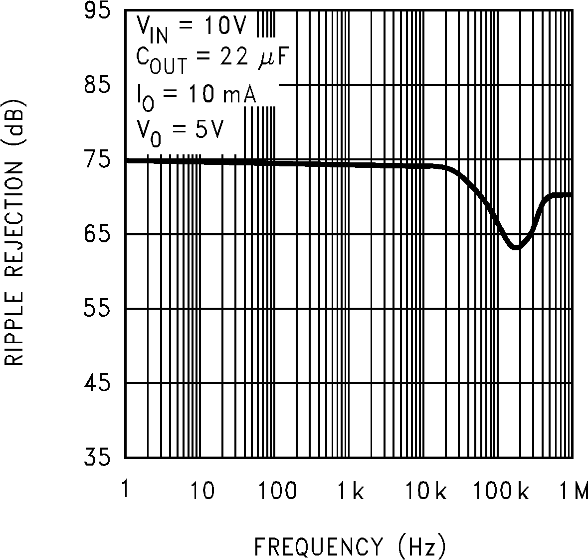 Figure 9. Ripple Rejection
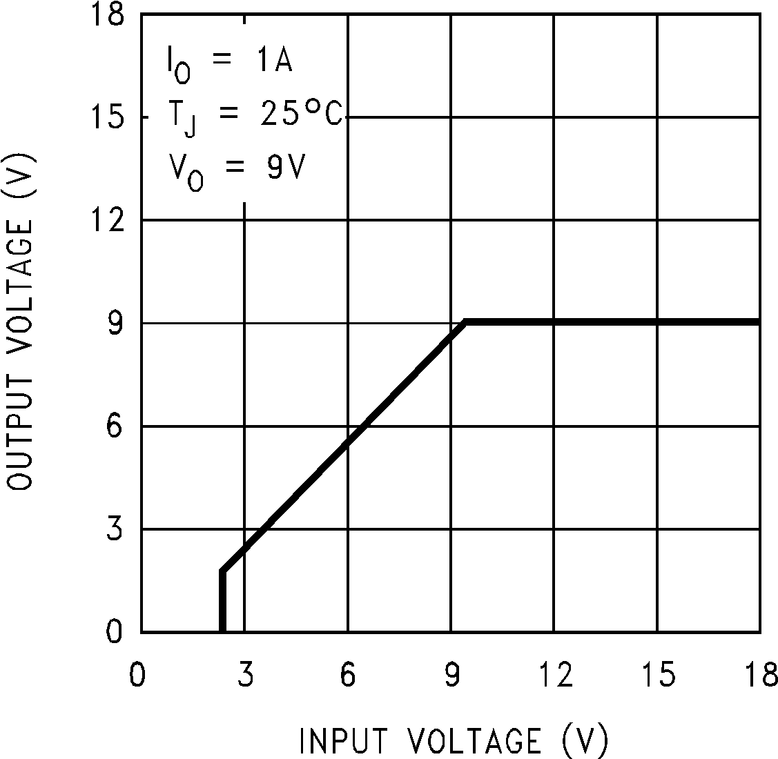 Figure 11. Low Voltage Behavior
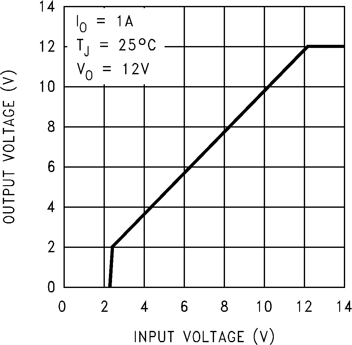 Figure 13. Low Voltage Behavior
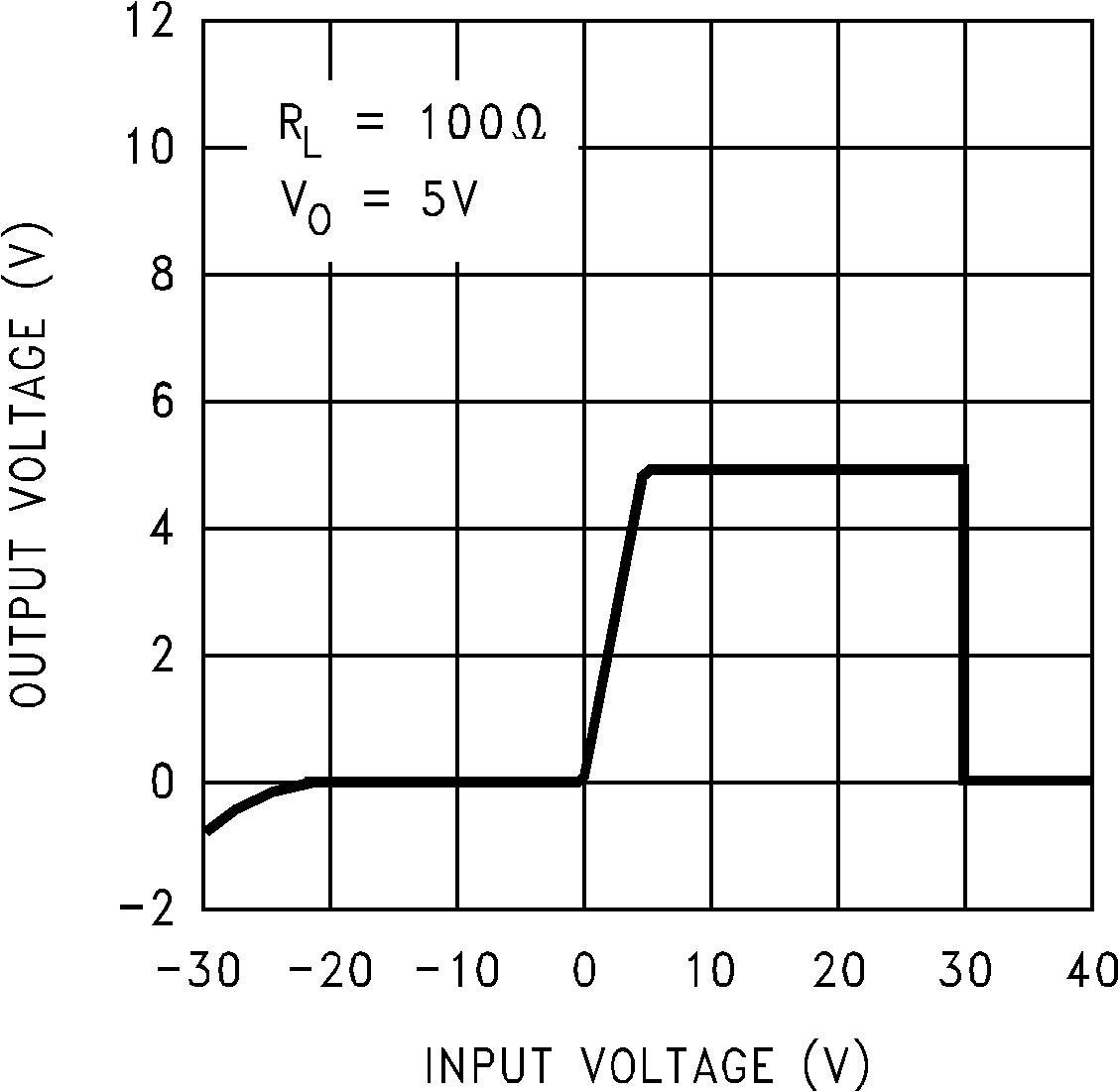 Figure 15. Output at Voltage Extremes
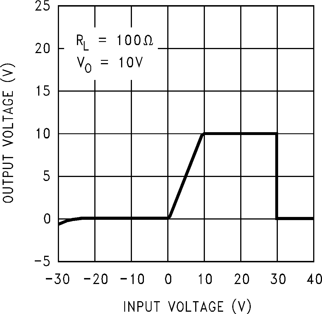 Figure 17. Output at Voltage Extremes
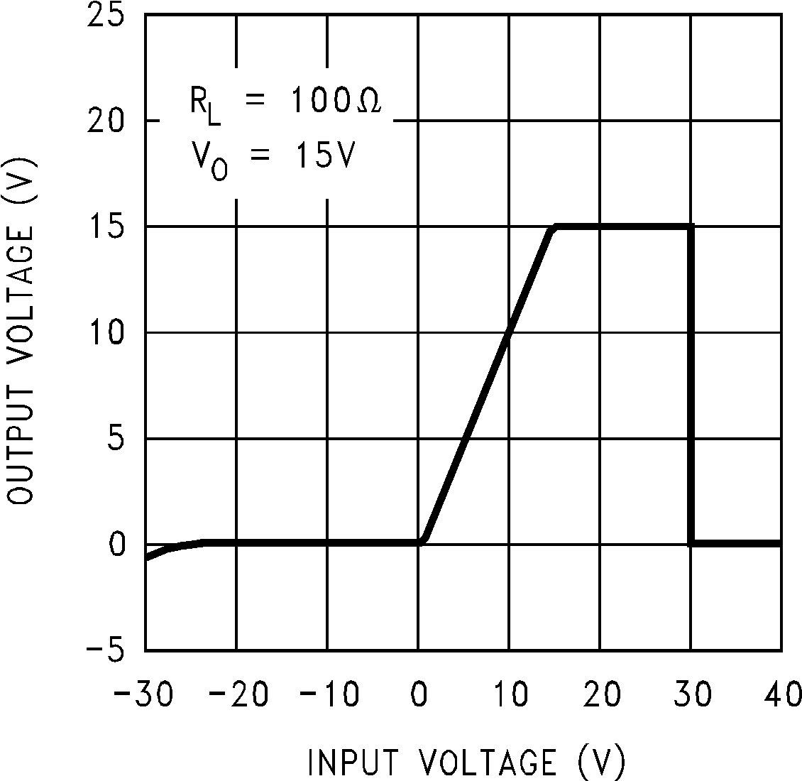 Figure 19. Output at Voltage Extremes
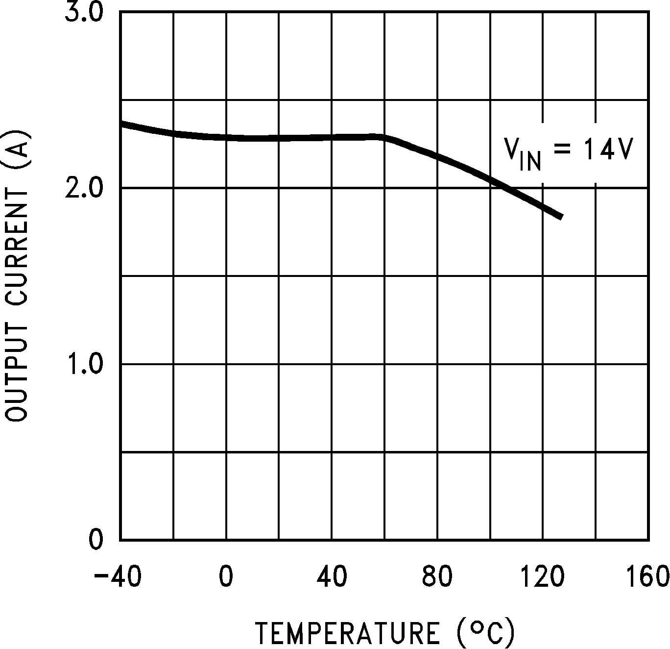 Figure 21. Peak Output Current
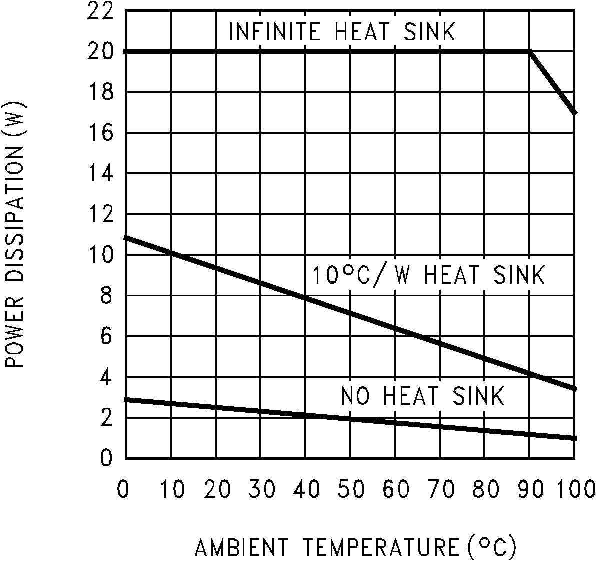 Figure 23. Maximum Power Dissipation (TO-220)
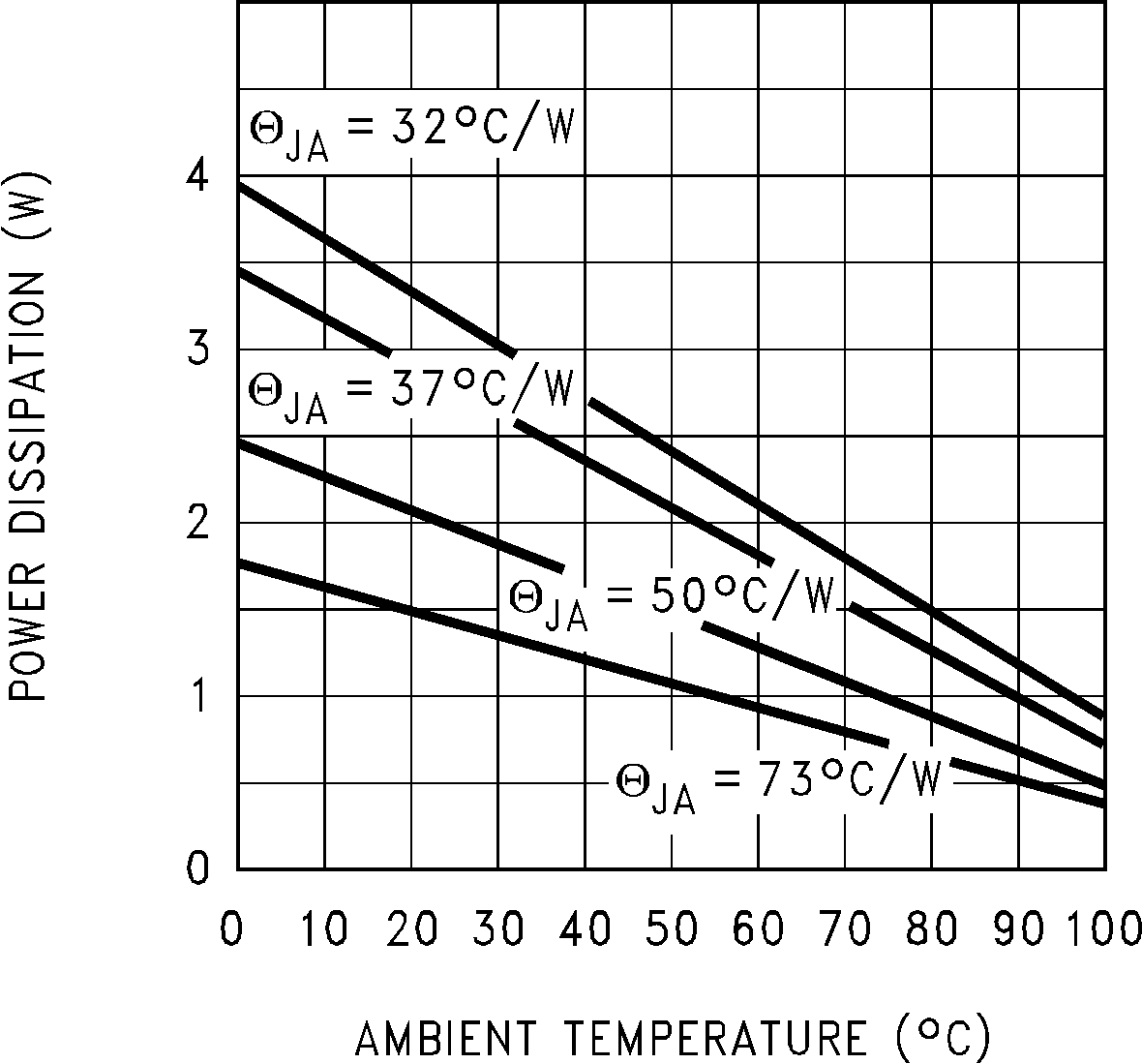 Figure 25. Maximum Power Dissipation (DDPAK/TO-263)
 Figure 6. Quiescent Current
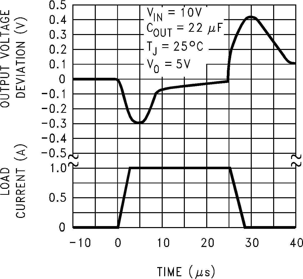 Figure 8. Load Transient Response
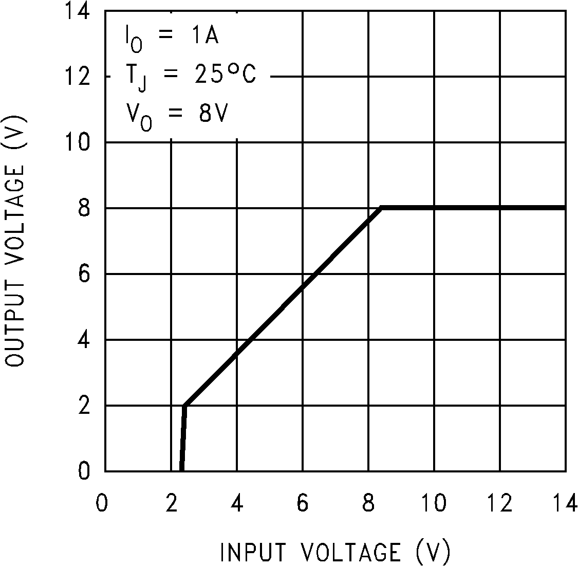 Figure 10. Low Voltage Behavior
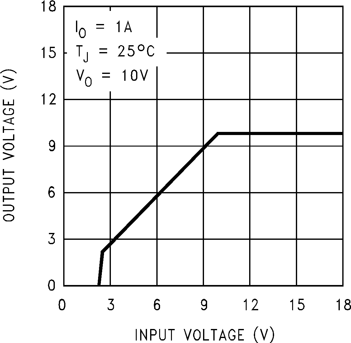 Figure 12. Low Voltage Behavior
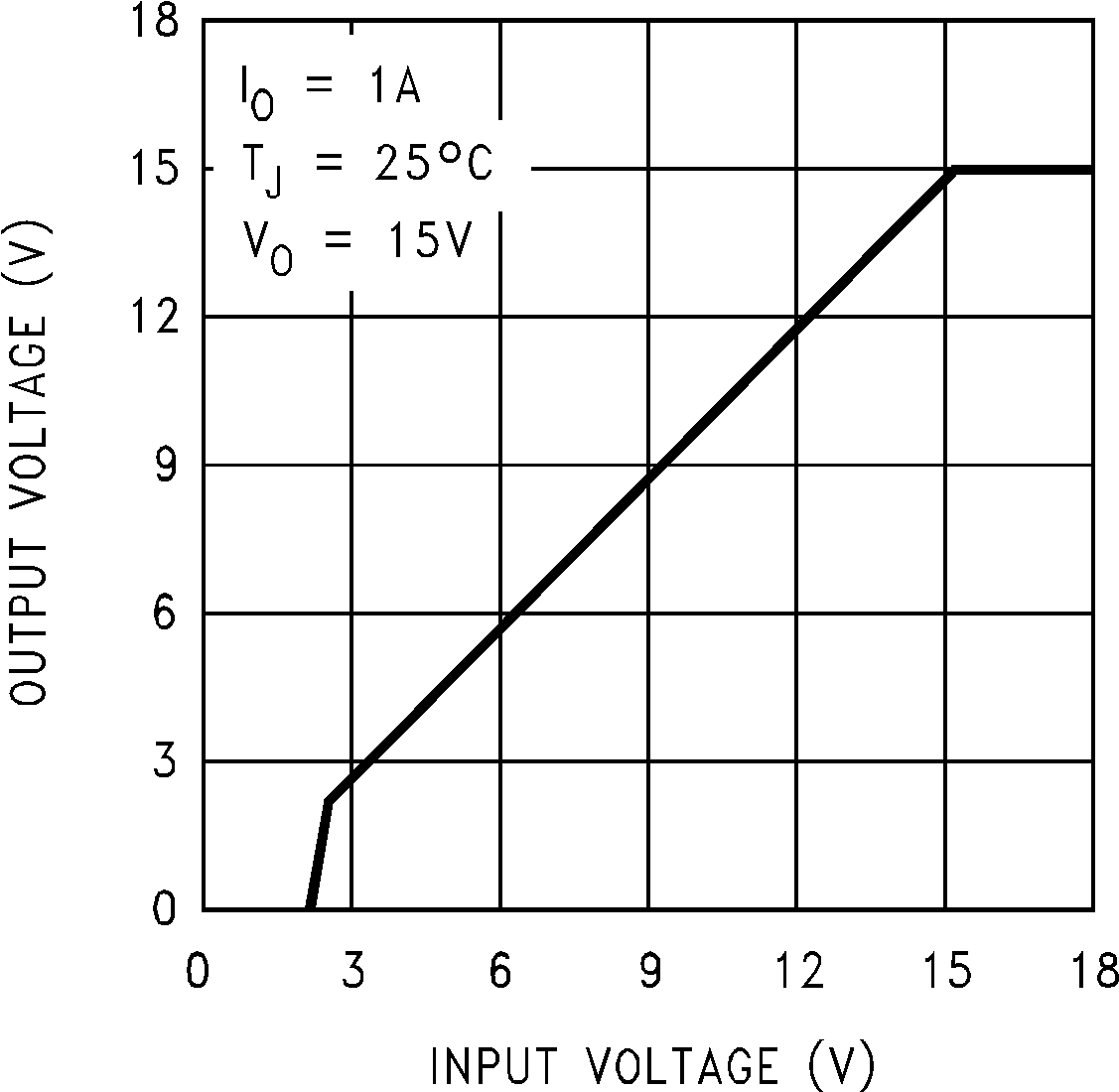 Figure 14. Low Voltage Behavior
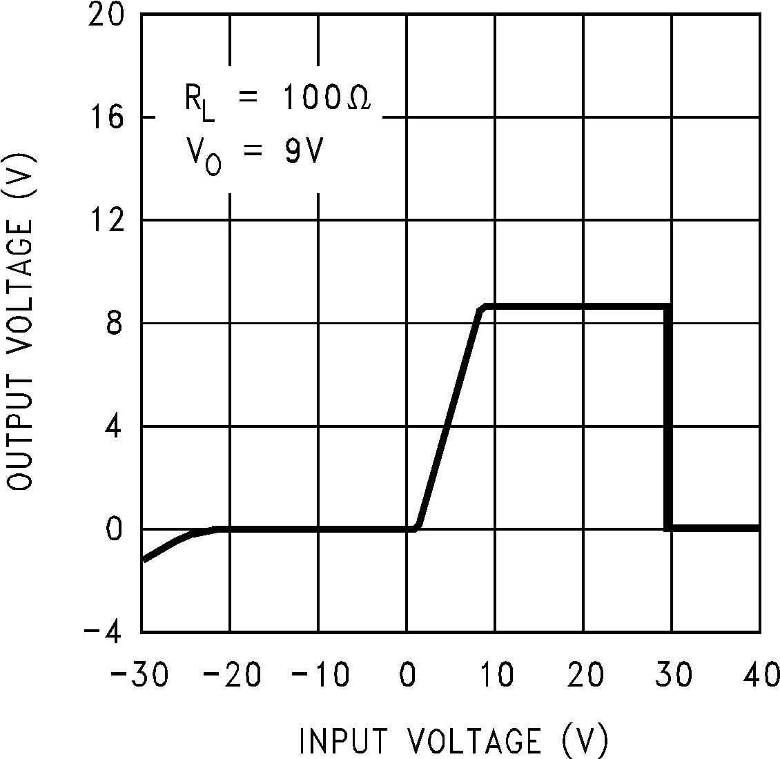 Figure 16. Output at Voltage Extremes
 Figure 18. Output at Voltage Extremes
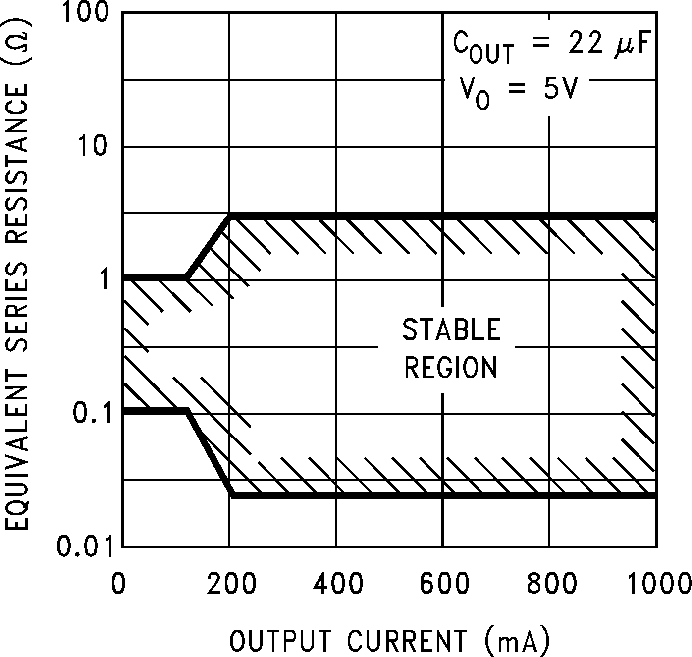 Figure 20. Output Capacitor ESR
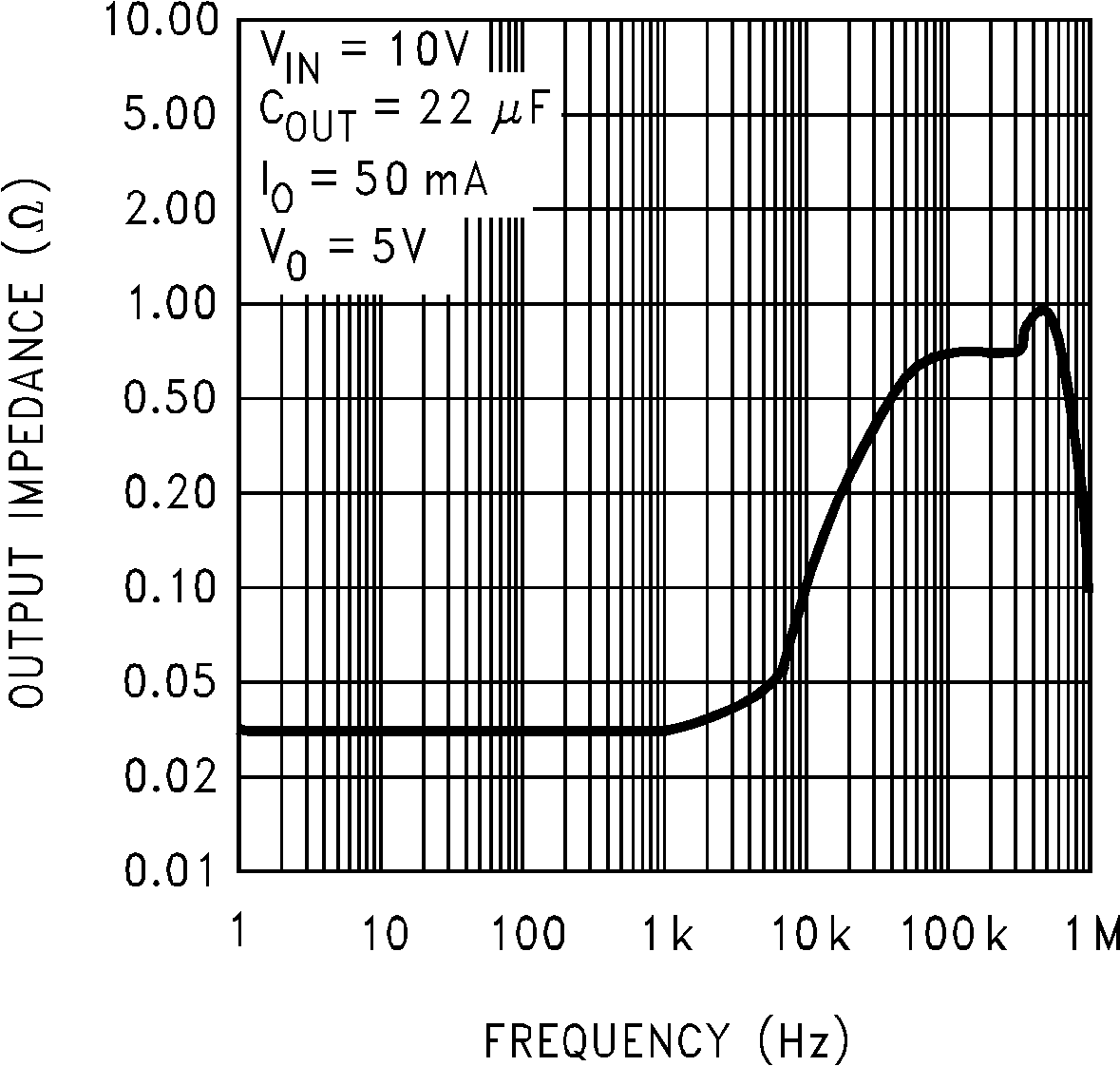 Figure 22. Output Impedance
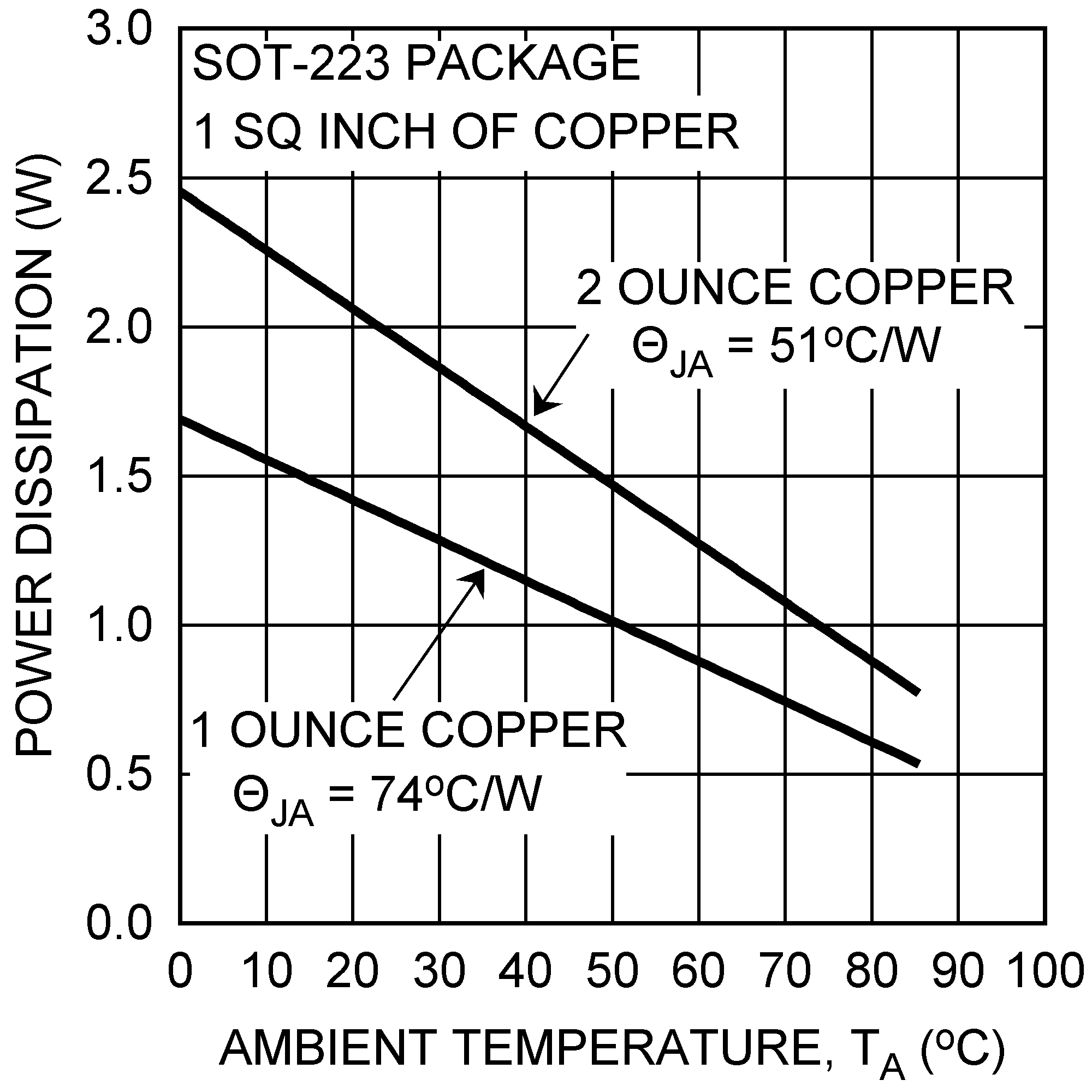 Figure 24. Maximum Power Dissipation (SOT-223)