SNVS769J March 2000 – December 2014 LM2940-N , LM2940C
PRODUCTION DATA.
- 1 Features
- 2 Applications
- 3 Description
- 4 Revision History
- 5 Pin Configuration and Functions
- 6 Specifications
- 7 Detailed Description
- 8 Application and Implementation
- 9 Power Supply Recommendations
- 10Layout
- 11Device and Documentation Support
- 12Mechanical, Packaging, and Orderable Information
封装选项
请参考 PDF 数据表获取器件具体的封装图。
机械数据 (封装 | 引脚)
- NDE|3
- NGN|8
- DCY|4
- KTT|3
- NEB|3
散热焊盘机械数据 (封装 | 引脚)
订购信息
10 Layout
10.1 Layout Guidelines
The dynamic performance of the LM2940 is dependent on the layout of the PCB. PCB layout practices that are adequate for typical LDOs may degrade the PSRR, noise, or transient performance of the LM2940. Best performance is achieved by placing CIN and COUT on the same side of the PCB as the LM2940, and as close as is practical to the package. The ground connections for CIN and COUT should be back to the LM2940 ground pin using as wide and short of a copper trace as is practical.
10.2 Layout Examples
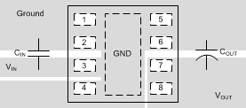 Figure 30. LM2940 WSON Layout
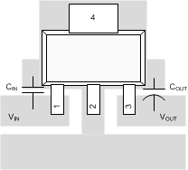 Figure 31. LM2940 SOT-223 Layout
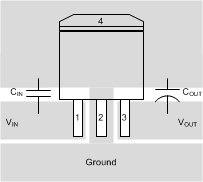 Figure 32. TO-263 Layout
10.3 Heatsinking
A heatsink may be required depending on the maximum power dissipation and maximum ambient temperature of the application. Under all possible operating conditions, the junction temperature must be within the range specified under Absolute Maximum Ratings.
To determine if a heatsink is required, the power dissipated by the regulator, PD, must be calculated.
Figure 33 shows the voltages and currents which are present in the circuit, as well as the formula for calculating the power dissipated in the regulator:
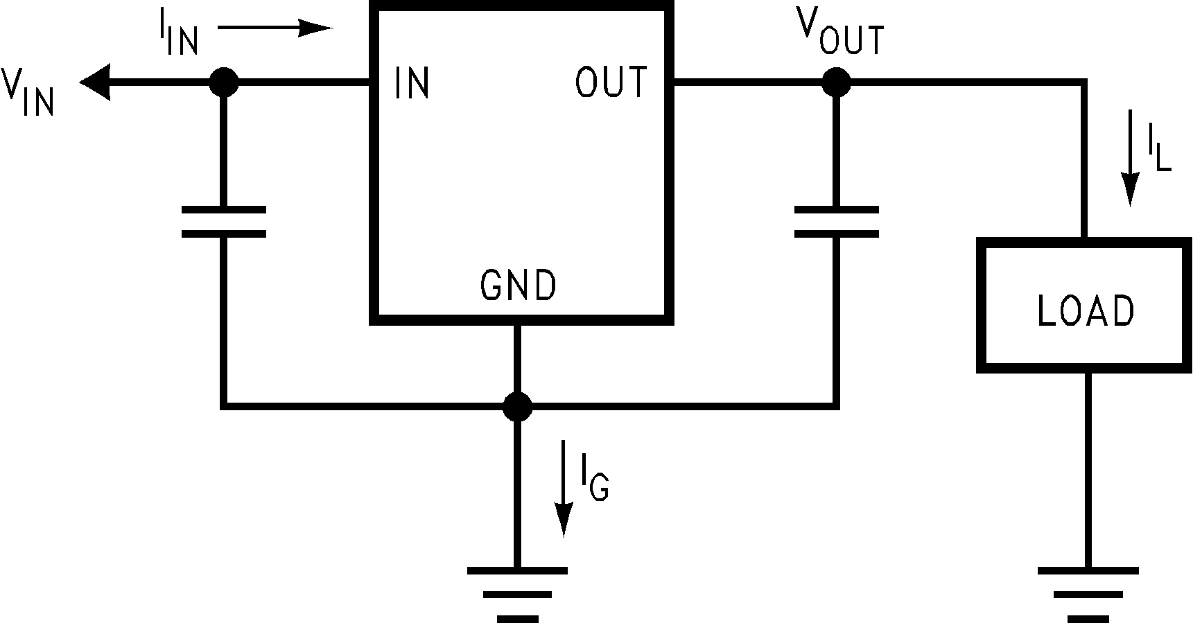
PD = (VIN − VOUT) IL + (VIN) IG
The next parameter which must be calculated is the maximum allowable temperature rise, TR(MAX). This is calculated by using the formula:
where
- TJ(MAX) is the maximum allowable junction temperature, which is 125°C for commercial grade parts.
- TA(MAX)is the maximum ambient temperature which will be encountered in the application.
Using the calculated values for TR(MAX) and PD, the maximum allowable value for the junction-to-ambient thermal resistance, RθJA, can now be found:
NOTE
If the maximum allowable value for RθJA is found to be ≥ 23.3°C/W for the TO-220 package (with a heatsink of 21.7°C/W RθSA), ≥ 40.9°C/W for the DDPAK/TO-263 package, or ≥ 59.3°C/W for the SOT-223 package, no heatsink is needed since the package alone will dissipate enough heat to satisfy these requirements.
If the calculated value for RθJA falls below these limits, a heatsink is required.
10.3.1 Heatsinking TO-220 Package Parts
The TO-220 can be attached to a typical heatsink, or secured to a copper plane on a PC board.
If a manufactured heatsink is to be selected, the value of heatsink-to-ambient thermal resistance, RθSA, must first be calculated:
where
- RθJC is defined as the thermal resistance from the junction to the surface of the case. A value of 3°C/W can be assumed for RθJC for this calculation.
- RθCS is defined as the thermal resistance between the case and the surface of the heatsink. The value of RθCS will vary from about 0.5°C/W to about 2.5°C/W (depending on method of attachment, insulator, etc.). If the exact value is unknown, 2°C/W should be assumed for RθCS.
When a value for RθSA is found using Equation 3, a heatsink must be selected that has a value that is less than or equal to this number.
RθSA is specified numerically by the heatsink manufacturer in the catalog, or shown in a curve that plots temperature rise vs power dissipation for the heatsink.