SNVS071C March 2000 – September 2015 LM2766
PRODUCTION DATA.
- 1 Features
- 2 Applications
- 3 Description
- 4 Revision History
- 5 Pin Configuration and Functions
- 6 Specifications
- 7 Parameter Measurement Information
- 8 Detailed Description
- 9 Application and Implementation
- 10Power Supply Recommendations
- 11Layout
- 12Device and Documentation Support
- 13Mechanical, Packaging, and Orderable Information
9 Application and Implementation
NOTE
Information in the following applications sections is not part of the TI component specification, and TI does not warrant its accuracy or completeness. TI’s customers are responsible for determining suitability of components for their purposes. Customers should validate and test their design implementation to confirm system functionality.
9.1 Application Information
The LM2766 provides a simple and efficient means of creating an output voltage level equal to twice that of the input voltage. Without the need of an inductor, the application solution size can be reduced versus the magnetic DC-DC converter solution.
9.2 Typical Application
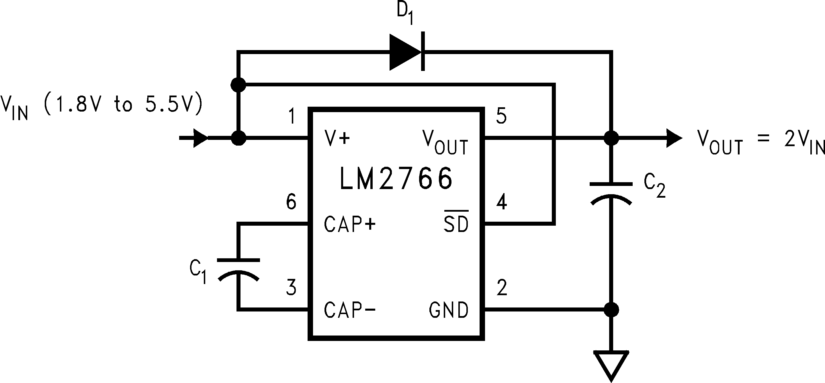
The main application of the LM2766 is to double the input voltage.
 Figure 11. LM2766 Typical Application
9.2.1 Design Requirements
For typical switched-capacitor voltage converter applications, use the parameters listed in Table 1.
Table 1. Design Parameters
| DESIGN PARAMETER | EXAMPLE VALUE |
|---|---|
| Minimum input voltage | 1.8 to 5.5 V |
| Output current (minimum), 2.5 V ≤ VIN ≤ 5.5 V | 20 mA |
| Output current (minimum), 1.8 V ≤ VIN ≤ 2.5 V | 10 mA |
| Switching frequency | 200 kHz (typical) |
9.2.2 Detailed Design Procedure
9.2.2.1 Positive Voltage Doubler
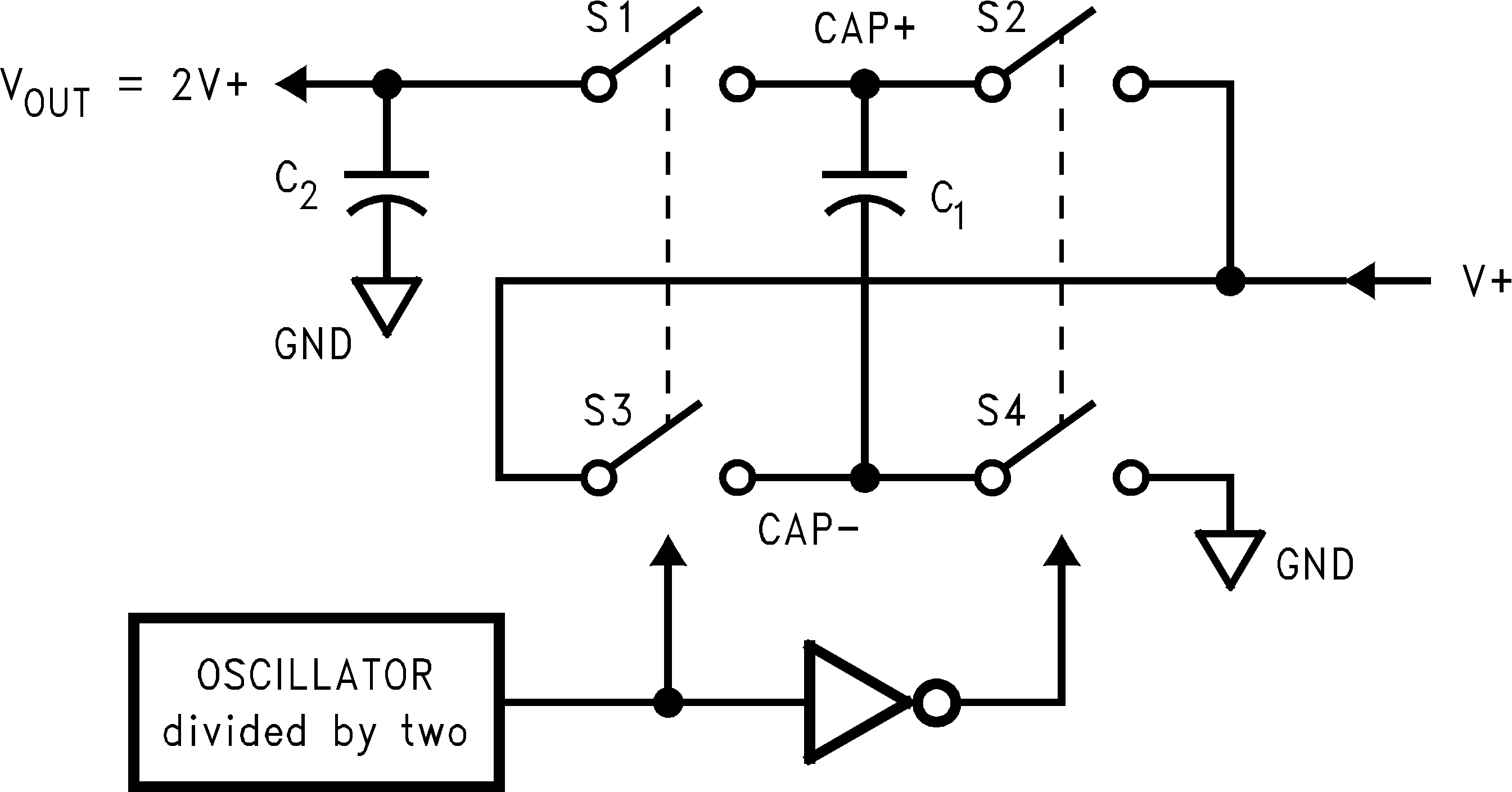
 Figure 12. Voltage Doubling Principle
The output characteristics of this circuit can be approximated by an ideal voltage source in series with a resistance. The voltage source equals 2 V+. The output resistance Rout is a function of the ON resistance of the internal MOSFET switches, the oscillator frequency, and the capacitance and ESR of C1 and C2. Because the switching current charging and discharging C1 is approximately twice the output current, the effect of the ESR of the pumping capacitor C1 is multiplied by four in the output resistance. The output capacitor C2 is charging and discharging at a current approximately equal to the output current, therefore, its ESR only counts once in the output resistance. A good approximation of Rout is:

where
- RSW is the sum of the ON resistance of the internal MOSFET switches shown in Figure 12.
The peak-to-peak output voltage ripple is determined by the oscillator frequency as well as the capacitance and ESR of the output capacitor C2:

High capacitance, low ESR capacitors can reduce both the output resistance and the voltage ripple.
The Schottky diode D1 is only needed to protect the device from turning on its own parasitic diode and potentially latching up. During start-up, D1 also quickly charges up the output capacitor to VIN minus the diode drop thereby decreasing the start-up time. Therefore, the Schottky diode D1 must have enough current carrying capability to charge the output capacitor at start-up, as well as a low forward voltage to prevent the internal parasitic diode from turning on. A Schottky diode like 1N5817 can be used for most applications. If the input voltage ramp is less than 10 V/ms, a smaller Schottky diode like MBR0520LT1 can be used to reduce the circuit size.
9.2.2.2 Capacitor Selection
As discussed in Positive Voltage Doubler, the output resistance and ripple voltage are dependent on the capacitance and ESR values of the external capacitors. The output voltage drop is the load current times the output resistance, and the power efficiency is

where
- IQ(V+) is the quiescent power loss of the device; and
- IL2ROUT is the conversion loss associated with the switch on-resistance, the two external capacitors and their ESRs.
The selection of capacitors is based on the specifications of the dropout voltage (which equals IOUT ROUT), the output voltage ripple, and the converter efficiency. Low ESR capacitors (Table 2) are recommended to maximize efficiency, reduce the output voltage drop and voltage ripple.
Table 2. Low ESR Capacitor Manufacturers
| MANUFACTURER | WEBSITE | CAPACITOR TYPE |
|---|---|---|
| Nichicon Corp. | www.nichicon.com | PL & PF series, through-hole aluminum electrolytic |
| AVX Corp. | www.avxcorp.com | TPS series, surface-mount tantalum |
| Sprague | www.vishay.com | 593D, 594D, 595D series, surface-mount tantalum |
| Sanyo | www.sanyovideo.com | OS-CON series, through-hole aluminum electrolytic |
| Murata | www.murata.com | Ceramic chip capacitors |
| Taiyo Yuden | www.t-yuden.com | Ceramic chip capacitors |
| Tokin | www.tokin.com | Ceramic chip capacitors |
9.2.2.3 Paralleling Devices
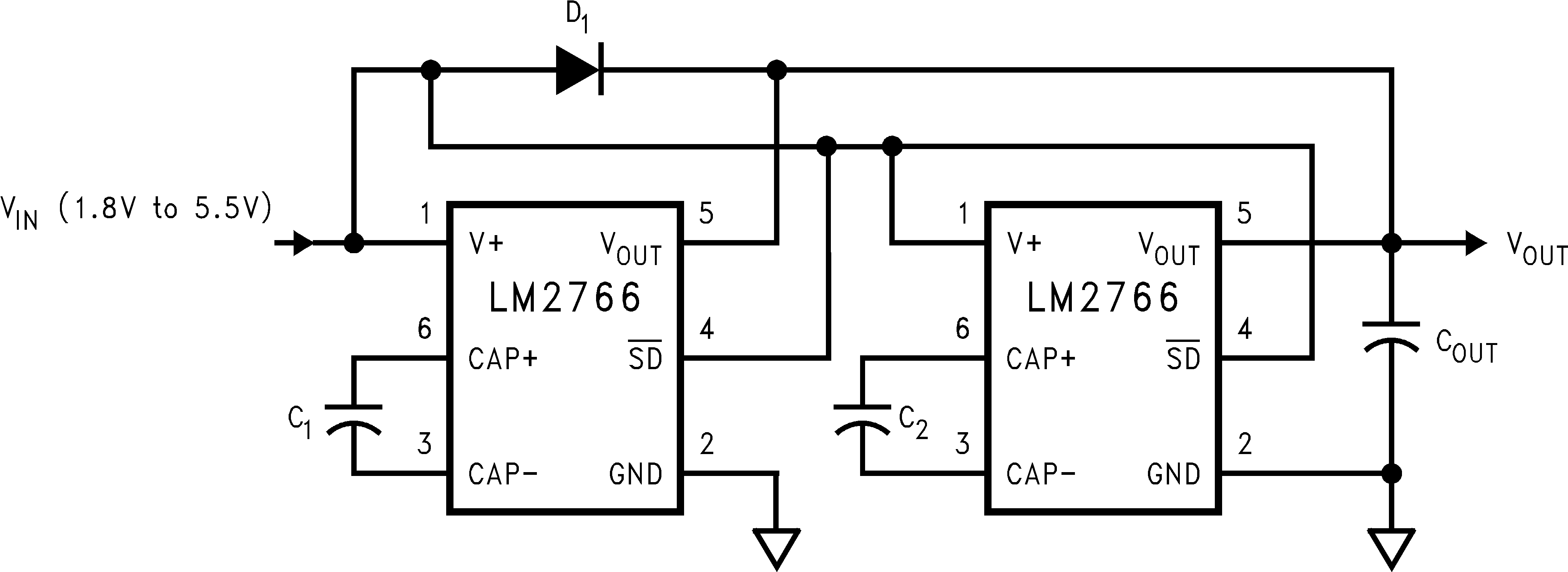
Any number of LM2766 devices can be paralleled to reduce the output resistance. Because there is no closed loop feedback, as found in regulated circuits, stable operation is assured. Each device must have its own pumping capacitor C1, while only one output capacitor COUT is needed as shown in Figure 13. The composite output resistance is:

 Figure 13. Lowering Output Resistance By Paralleling Devices
9.2.2.4 Cascading Devices
Cascading the several LM2766 devices is an easy way to produce a greater voltage (a two-stage cascade circuit is shown in Figure 14).
The effective output resistance is equal to the weighted sum of each individual device:
Note that increasing the number of cascading stages is practically limited because it significantly reduces the efficiency, increases the output resistance and output voltage ripple.
 Figure 14. Increasing Output Voltage By Cascading Devices
9.2.2.5 Regulating VOUT
It is possible to regulate the output of the LM2766 by use of a low dropout regulator (such as LP2980-5.0). The whole converter is depicted in Figure 15.
A different output voltage is possible by use of LP2980-3.3, LP2980-3.0, or LP2980-ADJ.
The following conditions must be satisfied simultaneously for worst case design:
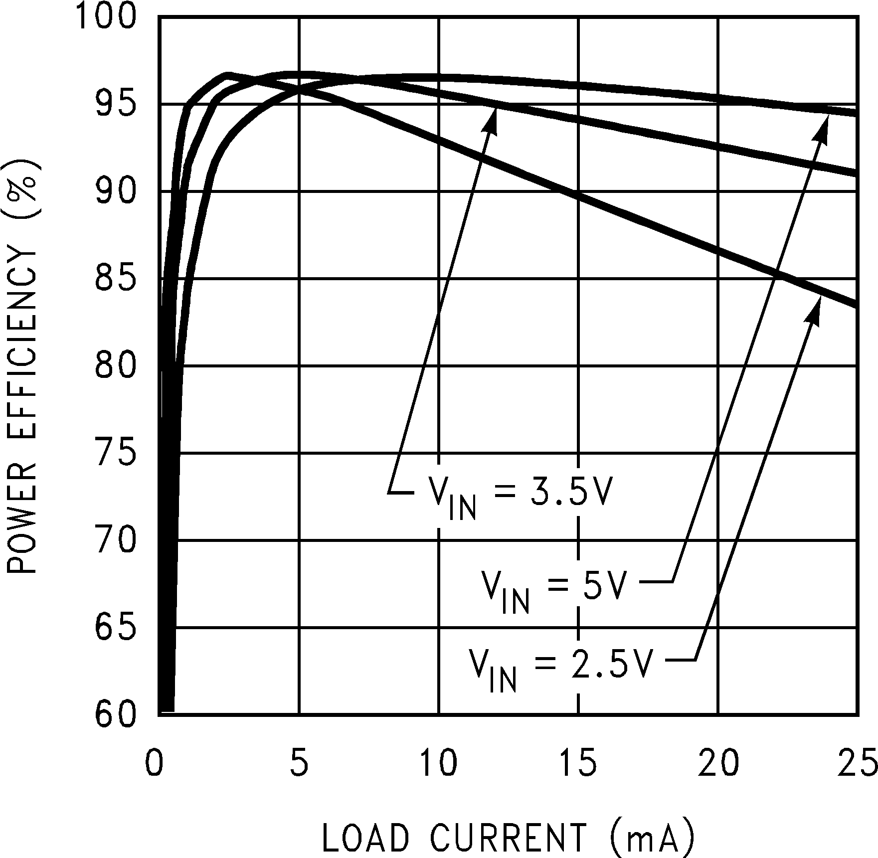
9.2.3 Application Curve

