SNVS487E December 2006 – January 2015 LM27313 , LM27313-Q1
PRODUCTION DATA.
- 1 Features
- 2 Applications
- 3 Description
- 4 Revision History
- 5 Pin Configuration and Functions
- 6 Specifications
- 7 Detailed Description
-
8 Application and Implementation
- 8.1 Application Information
- 8.2
Typical Applications
- 8.2.1
Application Circuit VIN=5.0 V, VOUT=12.0 V, Iload=250 mA
- 8.2.1.1 Design Requirements
- 8.2.1.2
Detailed Design Procedure
- 8.2.1.2.1 Selecting the External Capacitors
- 8.2.1.2.2 Selecting the Output Capacitor
- 8.2.1.2.3 Selecting the Input Capacitor
- 8.2.1.2.4 Feed-Forward Compensation
- 8.2.1.2.5 Selecting Diodes
- 8.2.1.2.6 Setting the Output Voltage
- 8.2.1.2.7 Duty Cycle
- 8.2.1.2.8 Inductance Value
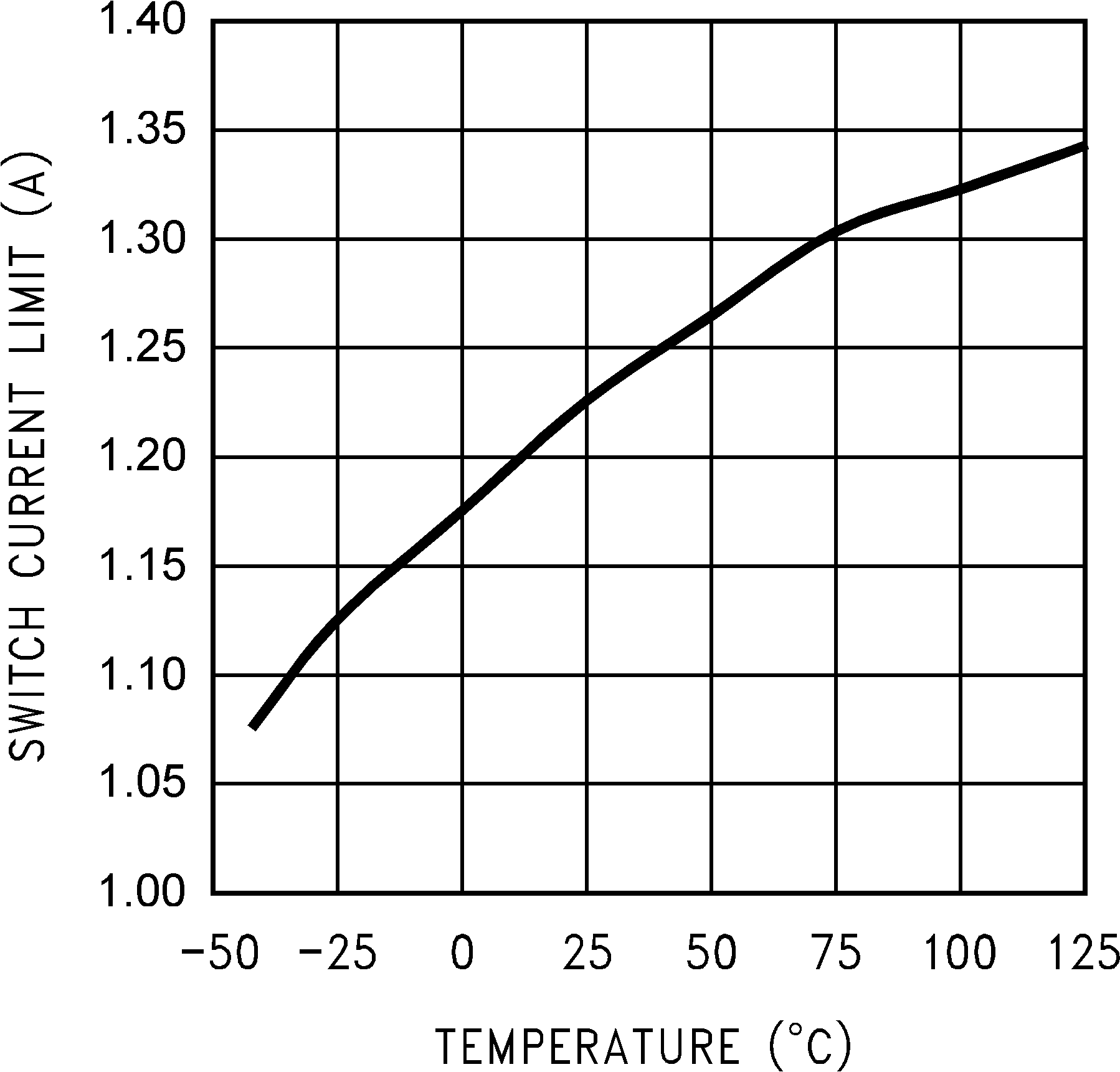
- 8.2.1.2.9 Maximum Switch Current
- 8.2.1.2.10 Calculating Load Current
- 8.2.1.2.11 Design Parameters VSW and ISW
- 8.2.1.2.12 Minimum Inductance
- 8.2.1.2.13 Inductor Suppliers
- 8.2.1.2.14 Shutdown Pin Operation
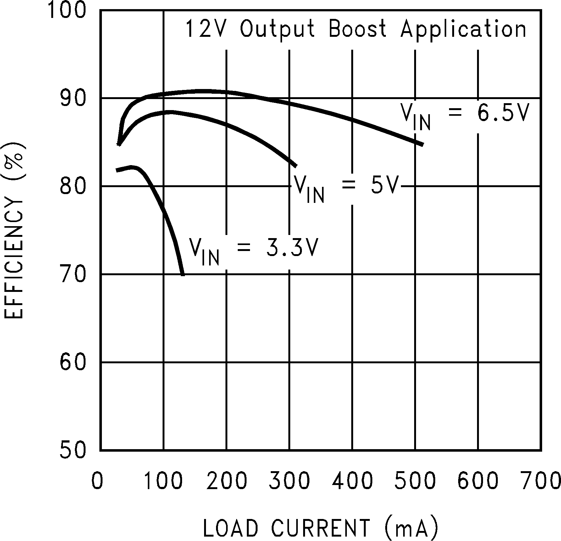
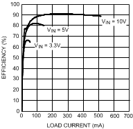
- 8.2.1.3 Application Curves
- 8.2.2 Application Circuit VIN=5.0V, VOUT=20.0V, Iload=150mA
- 8.2.1
Application Circuit VIN=5.0 V, VOUT=12.0 V, Iload=250 mA
- 9 Power Supply Recommendations
- 10Layout
- 11Device and Documentation Support
- 12Mechanical, Packaging, and Orderable Information
6 Specifications
6.1 Absolute Maximum Ratings(1)(2)
| MIN | MAX | UNIT | ||
|---|---|---|---|---|
| FB Pin Voltage | −0.4 | 6 | V | |
| SW Pin Voltage | −0.4 | 30 | V | |
| Input Supply Voltage | −0.4 | 14.5 | V | |
| Shutdown Input Voltage | (Survival) | −0.4 | 14.5 | V |
| Lead Temp. (Soldering, 5 s) | 300 | °C | ||
| Power Dissipation | Internally Limited | |||
| Storage temperature, Tstg | −65 | 150 | °C | |
(1) Stresses beyond those listed under Absolute Maximum Ratings may cause permanent damage to the device. These are stress ratings only, which do not imply functional operation of the device at these or any other conditions beyond those indicated under Recommended Operating Conditions. Exposure to absolute-maximum-rated conditions for extended periods may affect device reliability.
(2) If Military/Aerospace specified devices are required, please contact the Texas Instruments Sales Office/ Distributors for availability and specifications.
6.2 ESD Ratings: LM27313
| VALUE | UNIT | ||||
|---|---|---|---|---|---|
| V(ESD) | Electrostatic discharge | Human body model (HBM), per ANSI/ESDA/JEDEC JS-001, all pins(1) | ±2000 | V | |
| Charged device model (CDM), per JEDEC specification JESD22-C101, all pins(2) | ±1000 | ||||
(1) JEDEC document JEP155 states that 500-V HBM allows safe manufacturing with a standard ESD control process.
(2) JEDEC document JEP157 states that 250-V CDM allows safe manufacturing with a standard ESD control process.
6.3 ESD Ratings: LM27313-Q1
| VALUE | UNIT | |||||
|---|---|---|---|---|---|---|
| V(ESD) | Electrostatic discharge | Human body model (HBM), per AEC Q100-002(1) | ±2000 | V | ||
| Charged device model (CDM), per AEC Q100-011 | Corner pins (1, 3, 4, and 5) | ±1000 | ||||
| Other pins | ±1000 | |||||
(1) AEC Q100-002 indicates HBM stressing is done in accordance with the ANSI/ESDA/JEDEC JS-001 specification.
6.4 Recommended Operating Conditions
| MIN | NOM | MAX | UNIT | |
|---|---|---|---|---|
| VIN | 2.7 | 14 | V | |
| VSW(MAX) | 30 | V | ||
| VSHDN | 0 | VIN | V | |
| Junction Temperature, TJ | –40 | 125 | °C |
6.5 Thermal Information
| THERMAL METRIC(1) | LM27313, LM27313-Q1 | UNIT | |
|---|---|---|---|
| DBV | |||
| 5 PINS | |||
| RθJA | Junction-to-ambient thermal resistance | 166.3 | °C/W |
| RθJC(top) | Junction-to-case (top) thermal resistance | 71.8 | |
| RθJB | Junction-to-board thermal resistance | 28.1 | |
| ψJT | Junction-to-top characterization parameter | 2.1 | |
| ψJB | Junction-to-board characterization parameter | 27.7 | |
| RθJC(bot) | Junction-to-case (bottom) thermal resistance | N/A | |
(1) For more information about traditional and new thermal metrics, see the IC Package Thermal Metrics application report, SPRA953.
6.6 Electrical Characteristics
Unless otherwise specified: VIN = 5 V, VSHDN = 5 V, IL = 0 mA, and TJ = 25°C. Minimum and Maximum limits are ensured through test, design, or statistical correlation. Typical values represent the most likely parametric norm at TJ = 25°C, and are provided for reference purposes only.| PARAMETER | TEST CONDITIONS | MIN | TYP | MAX | UNIT | |
|---|---|---|---|---|---|---|
| VIN | Input Voltage | −40°C ≤ TJ ≤ +125°C | 2.7 | 14 | V | |
| ISW | Switch Current Limit | See(1) | 0.80 | 1.25 | A | |
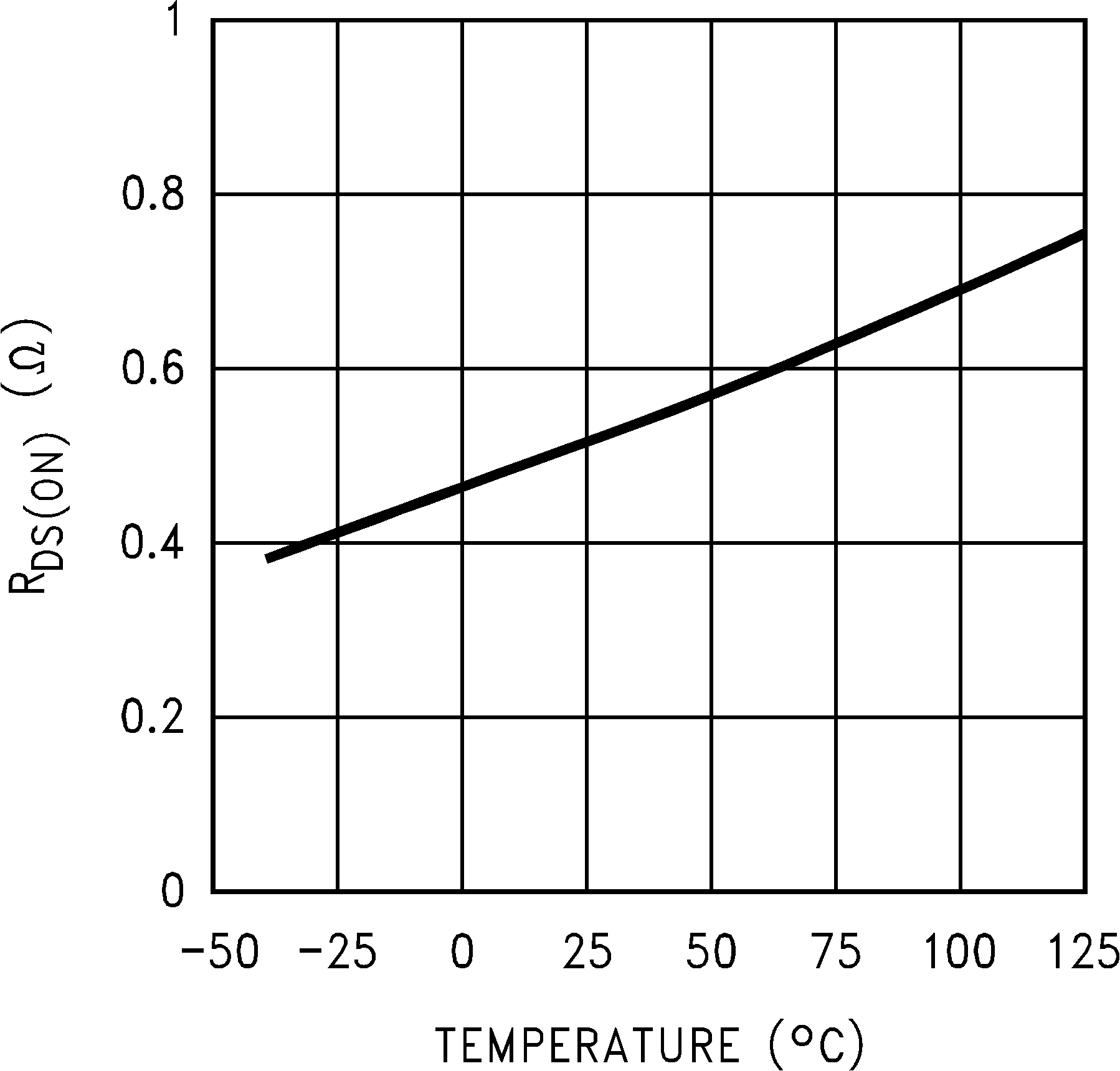
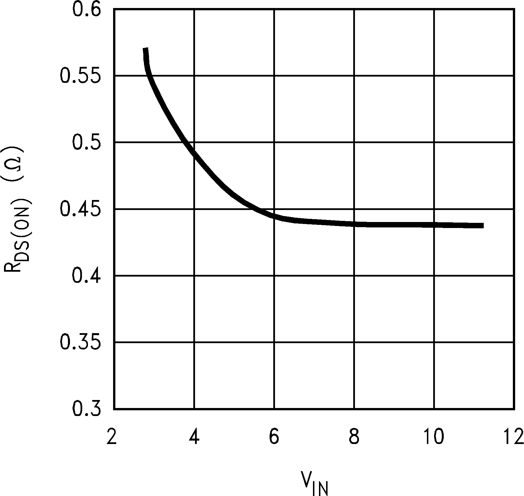
| RDS(ON) | Switch ON Resistance | ISW = 100 mA | 500 | 650 | mΩ | |
| VSHDN(TH) | Shutdown Threshold | Device ON, −40°C ≤ TJ ≤ +125°C | 1.5 | V | ||
| Device OFF, −40°C ≤ TJ ≤ +125°C | 0.50 | |||||
| ISHDN | Shutdown Pin Bias Current | VSHDN = 0 | 0 | µA | ||
| VSHDN = 5 V | 0 | 2 | ||||
| VSHDN = 5 V, −40°C ≤ TJ ≤ +125°C | ||||||
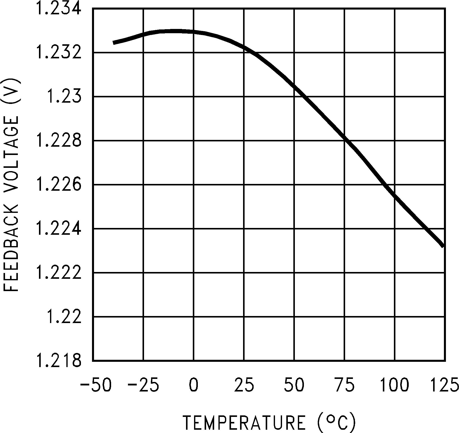
| VFB | Feedback Pin Reference Voltage | VIN = 3 V | 1.230 | V | ||
| VIN = 3 V, −40°C ≤ TJ ≤ +125°C | 1.205 | 1.255 | ||||
| IFB | Feedback Pin Bias Current | VFB = 1.23 V | 60 | nA | ||
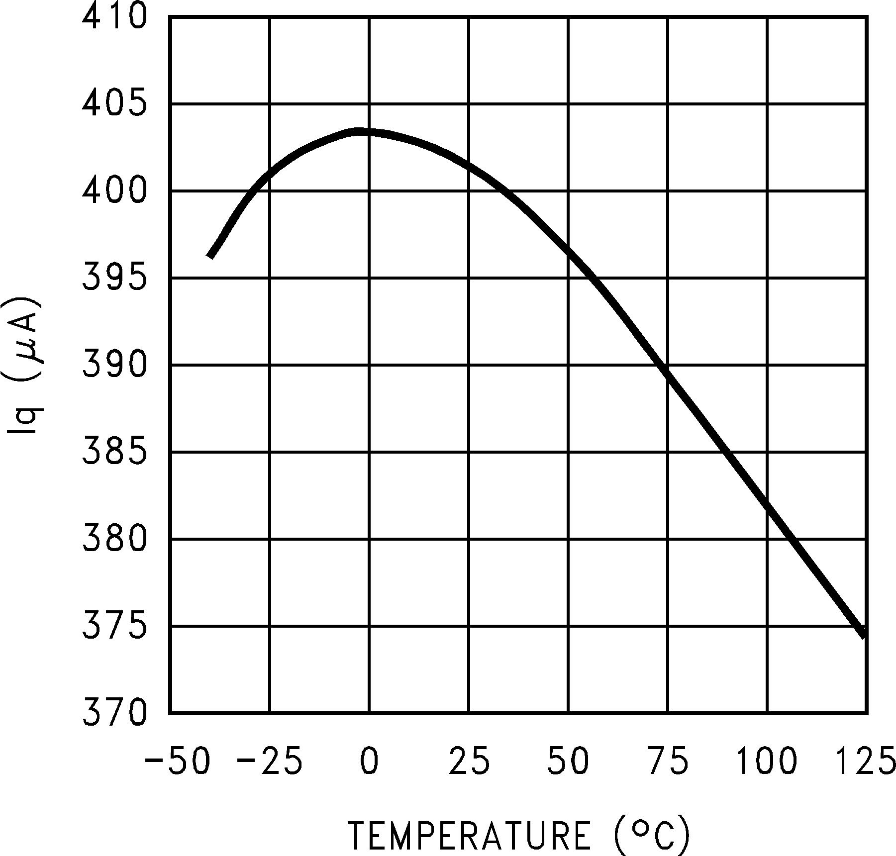
| IQ | Quiescent Current | VSHDN = 5 V, Switching | 2.1 | mA | ||
| VSHDN = 5 V, Switching, −40°C ≤ TJ ≤ +125°C | 3.0 | |||||
| VSHDN = 5 V, Not Switching | 400 | µA | ||||
| VSHDN = 5 V, Not Switching, −40°C ≤ TJ ≤ +125°C | 500 | |||||
| VSHDN = 0 | 0.024 | 1 | ||||
| ΔVFB/ΔVIN | FB Voltage Line Regulation | 2.7 V ≤ VIN ≤ 14 V | 0.02 | %/V | ||
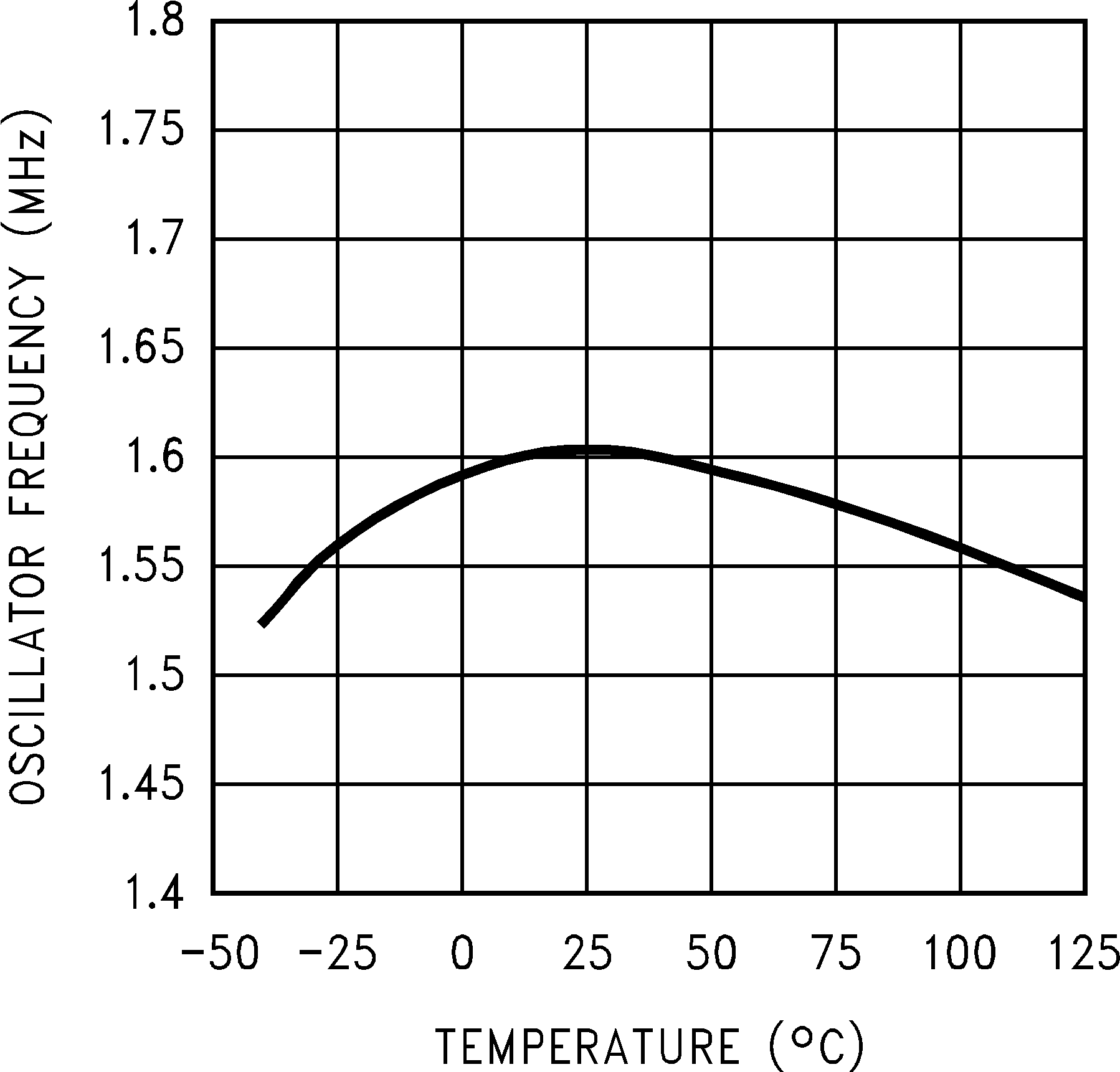
| fSW | Switching Frequency | 1.6 | MHz | |||
| −40°C ≤ TJ ≤ +125°C | 1.15 | 1.90 | ||||
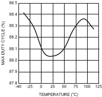
| DMAX | Maximum Duty Cycle | 88% | ||||
| −40°C ≤ TJ ≤ +125°C | 80% | |||||
| IL | Switch Leakage | Not Switching, VSW = 5 V | 1 | µA | ||
(1) Switch current limit is dependent on duty cycle. Limits shown are for duty cycles ≤ 50%. See Figure 15.
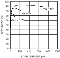
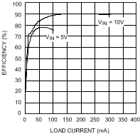
6.7 Typical Characteristics
Unless otherwise specified: VIN = 5 V, SHDN pin is tied to VIN, TJ = 25°C.