SNVS191F November   2002  – October 2016 LM2705

PRODUCTION DATA.  

  1. Features
  2. Applications
  3. Description
  4. Revision History
  5. Pin Configuration and Functions
  6. Specifications
    1. 6.1 Absolute Maximum Ratings
    2. 6.2 ESD Ratings
    3. 6.3 Recommended Operating Conditions
    4. 6.4 Thermal Information
    5. 6.5 Electrical Characteristics
    6. 6.6 Typical Characteristics
  7. Detailed Description
    1. 7.1 Overview
    2. 7.2 Functional Block Diagram
    3. 7.3 Feature Description
    4. 7.4 Device Functional Modes
  8. Application and Implementation
    1. 8.1 Application Information
    2. 8.2 Typical Application
      1. 8.2.1 Design Requirements
      2. 8.2.2 Detailed Design Procedure
        1. 8.2.2.1 Inductor Selection - Boost Regulator
        2. 8.2.2.2 Inductor Selection - SEPIC Regulator
        3. 8.2.2.3 Diode Selection
        4. 8.2.2.4 Capacitor Selection
      3. 8.2.3 Application Curves
    3. 8.3 Additional Applications
  9. Power Supply Recommendations
  10. 10Layout
    1. 10.1 Layout Guidelines
    2. 10.2 Layout Example
  11. 11Device and Documentation Support
    1. 11.1 Device Support
      1. 11.1.1 Third-Party Products Disclaimer
    2. 11.2 Receiving Notification of Documentation Updates
    3. 11.3 Community Resources
    4. 11.4 Trademarks
    5. 11.5 Electrostatic Discharge Caution
    6. 11.6 Glossary
  12. 12Mechanical, Packaging, and Orderable Information

封装选项

机械数据 (封装 | 引脚)
散热焊盘机械数据 (封装 | 引脚)
订购信息

Pin Configuration and Functions

DBV Package
5-Pin SOT-23
Top View
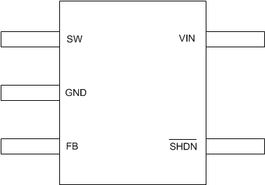
LM2705 20039702.gif

Pin Functions

PIN TYPE DESCRIPTION
NO. NAME
1 SW Input Power switch input. This is the drain of the internal NMOS power switch. Minimize the metal trace area connected to this pin to minimize EMI.
2 GND Ground - tie directly to ground plane.
3 FB Input Output voltage feedback input — set the output voltage by selecting values for R1 and R2 using: R1 = R2 × (VOUT / 1.237 V) –1
4 SHDN Input Active low shutdown - drive this pin to > 1.1 V to enable the device. Drive this pin to < 0.3 V to lace the device in a low-power shutdown.
5 VIN Input Analog and power input supply pin