ZHCSD82C January 2015 – November 2017 LM26480-Q1
PRODUCTION DATA.
- 1 特性
- 2 应用
- 3 说明
- 4 修订历史记录
- 5 Device Comparison Tables
- 6 Pin Configuration and Functions
-
7 Specifications
- 7.1 Absolute Maximum Ratings
- 7.2 ESD Ratings
- 7.3 Recommended Operating Conditions: Bucks
- 7.4 Thermal Information
- 7.5 General Electrical Characteristics
- 7.6 Low Dropout Regulators, LDO1 and LDO2
- 7.7 Buck Converters SW1, SW2
- 7.8 I/O Electrical Characteristics
- 7.9 Power-On Reset Threshold/Function (POR)
- 7.10 Typical Characteristics — LDO
- 7.11 Typical Characteristics — Buck 2.8 V to 5.5 V
- 7.12 Typical Characteristics — Bucks 1 and 2
- 7.13 Typical Characteristics — Buck 3.6 V
-
8 Detailed Description
- 8.1 Overview
- 8.2 Functional Block Diagram
- 8.3
Feature Description
- 8.3.1
DC-DC Converters
- 8.3.1.1 Linear Low Dropout Regulators (LDOs)
- 8.3.1.2
SW1, SW2: Synchronous Step-Down Magnetic DC-DC Converters
- 8.3.1.2.1 Functional Description
- 8.3.1.2.2 Circuit Operation Description
- 8.3.1.2.3 PWM Operation
- 8.3.1.2.4 Internal Synchronous Rectification
- 8.3.1.2.5 Current Limiting
- 8.3.1.2.6 PFM Operation
- 8.3.1.2.7 SW1, SW2 Control
- 8.3.1.2.8 Shutdown Mode
- 8.3.1.2.9 Soft Start
- 8.3.1.2.10 Low Dropout Operation
- 8.3.1.2.11 Flexible Power-On Reset (Power Good with Delay)
- 8.3.1.2.12 Undervoltage Lockout
- 8.3.1
DC-DC Converters
- 8.4 Device Functional Modes
-
9 Application and Implementation
- 9.1 Application Information
- 9.2
Typical Application
- 9.2.1 Design Requirements
- 9.2.2 Detailed Design Procedure
- 9.2.3 Application Curves
- 10Power Supply Recommendations
- 11Layout
- 12器件和文档支持
- 13机械、封装和可订购信息
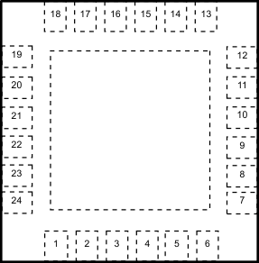
6 Pin Configuration and Functions
RTW Package
24-Pin WQFN
Top View

Pin Functions
| PIN | I/O | TYPE(1) | DESCRIPTION | |
|---|---|---|---|---|
| NO. | NAME | |||
| 1 | VINLDO12 | I | P | Analog power for internal functions (VREF, BIAS, I2C, Logic) |
| 2 | SYNC | I | G/(D) | Frequency synchronization pin, which allows the user to connect an external clock signal to synchronize the PMIC internal oscillator. Default OFF and must be grounded when not used. |
| 3 | NPOR | O | D | nPOR Power on reset pin for both Buck1 and Buck 2. Open drain logic output 100-kΩ pullup resistor. nPOR is pulled to ground when the voltages on these supplies are not good. See Flexible Power-On Reset (Power Good with Delay) for more information. |
| 4 | GND_SW1 | G | G | Buck1 NMOS power ground |
| 5 | SW1 | O | P | Buck1 switcher output pin |
| 6 | VIN1 | I | P | Power in from either DC source or battery to Buck1 |
| 7 | ENSW1 | I | D | Enable pin for Buck1 switcher, a logic HIGH enables Buck1. Pin cannot be left floating. |
| 8 | FB1 | I | A | Buck1 input feedback terminal |
| 9 | GND_C | G | G | Non-switching core ground pin |
| 10 | AVDD | I | P | Analog Power for Buck converters |
| 11 | FB2 | I | A | Buck2 input feedback terminal |
| 12 | ENSW2 | I | D | Enable pin for Buck2 switcher, a logic HIGH enables Buck2. Pin cannot be left floating. |
| 13 | VIN2 | I | P | Power in from either DC source or Battery to Buck2 |
| 14 | SW2 | O | P | Buck2 switcher output pin |
| 15 | GND_SW2 | G | G | Buck2 NMOS |
| 16 | ENLDO2 | I | D | LDO2 enable pin, a logic HIGH enables LDO2. Pin cannot be left floating. |
| 17 | ENLDO1 | I | D | LDO1 enable pin, a logic HIGH enables LDO1. Pin cannot be left floating. |
| 18 | GND_L | G | G | LDO ground |
| 19 | VINLDO1 | I | P | Power in from either DC source or battery to LDO1 |
| 20 | LDO1 | O | P | LDO1 Output |
| 21 | FBL1 | I | A | LDO1 feedback terminal |
| 22 | FBL2 | I | A | LDO2 feedback terminal |
| 23 | LDO2 | O | P | LDO output |
| 24 | VINLDO2 | I | P | Power in from either DC source or battery to LDO2. |
| DAP | DAP | G | G | Connection is not necessary for electrical performance, but it is recommended for better thermal dissipation. |
(1) A: Analog Pin, G: Ground Pin, P: Power Pin, I: Input Pin, O: Output Pin, D: Digital.